【Inkjet】🧪 05. GF180 Inkjet Driver Design Exploration (Part 2)
The Viable Point of an HV Driver Array Assuming 300 dpi
In the design exploration of an inkjet driver IC using the GF180MCU open PDK,
it was previously confirmed that a 400 dpi array is structurally infeasible
due to DNWELL constraints.
Based on that conclusion, this article examines:
How far an HV driver array can be considered a viable implementation target
when the design condition is fixed at 300 dpi
All discussion is organized based on actual GDS layout results.
This article is the concluding results chapter in the following series:
- Part 1: GF180 Inkjet Driver Design Exploration
https://zenn.dev/samizo_aitl/articles/024_gf180-inkjet-driver - Part 2: The Limit of 400 dpi and the Practical Reality of 300 dpi
(GDS-based confirmation that 400 dpi is structurally infeasible due to DNWELL constraints)
In the previous article, we reached the following conclusion:
With GF180MCU and DNWELL-based isolation,
a 400 dpi (63.5 µm) inkjet driver is structurally infeasible.
This article builds on that result and clarifies:
When the design condition is fixed at 300 dpi (~85 µm),
to what extent an HV driver array becomes a viable implementation target.
🎯 Why Fix the Design at 300 dpi
The pitch at 300 dpi is:
- 25.4 mm / 300 ≈ 84.7 µm
This is the smallest class of pitch that can simultaneously satisfy
the dominant constraints of GF180 HVMOS structures:
- DNWELL enclosure requirements
- Drift regions of high-voltage devices
- Guard rings and isolation margins
What mattered in the 400 dpi exploration was not:
“How much can we squeeze?”
but rather:
“Where does the realistic solution begin?”
That boundary was determined at the GDS level.
300 dpi represents that confirmed viable point.
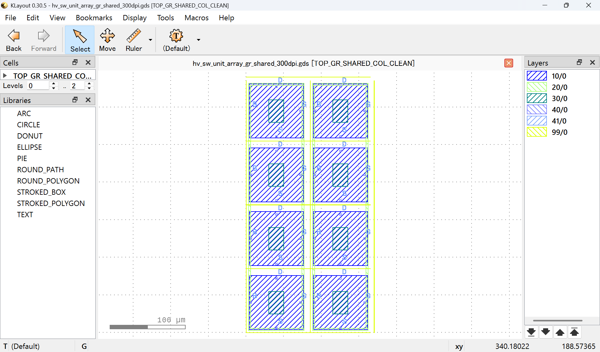
🧩 HV_SW_UNIT Array Dedicated to 300 dpi
At 300 dpi, the following design policies were adopted:
- DPI is no longer parameterized
→ Fixed at 300 dpi - Guard rings inside each HV_SW_UNIT are eliminated
- Column-wise shared guard rings are placed only at the array perimeter
- DNWELL continuity is treated as the highest priority
In the array-generation code, the essential change is effectively
limited to the pitch specification:
pitch_x = um(85.0, layout.dbu)  # 300 dpi
pitch_y = um(85.0, layout.dbu)
Structures that collapsed at 400 dpi now fall into a range where
they can be placed naturally and without forcing at 300 dpi.
※ This array evaluation assumes the most restrictive DNWELL isolation conditions
and uses an NMOS-dominant 4×2 configuration as the minimal evaluation block.
As a result, viability at 300 dpi is confirmed not for an idealized single cell,
but under effective physical conditions including the array interior.
🔍 What Was Confirmed in GDS
By generating and inspecting the 300 dpi array GDS, the following became clear:
- DNWELL enclosures fit naturally without distortion
- Guard rings no longer act as obstacles, but function as
meaningful isolation structures - Routing margin for power and signals becomes visible between units
- The array transitions from a “placement experiment” to something that can be read as
a foundational IC structure
The key point is this:
300 dpi is not “possible with clever tricks,”
but “already viable as a premise.”
At 400 dpi, a sense of structural strain remained no matter what was removed.
At 300 dpi, design decisions can be made naturally.
🚪 300 dpi Is Not the Goal, but It Is the Entrance
Of course, reducing the pitch to 300 dpi does not immediately deliver:
- Product-level reliability
- A fully functional driver circuit
- Pad / ESD / test structures
However, by clearing the heaviest physical constraints:
- DNWELL
- High-voltage devices
- Guard rings
- Array pitch
it can be said that:
The design has earned the right to move forward.
🛠 Next Steps Assuming 300 dpi
With 300 dpi as a fixed premise, the next phase becomes realistic:
- Replacing HV_SW_UNIT placeholders with real devices
- Substituting actual GF180 HV MOS devices
- Designing the power and GND routing backbone
- Clear separation of HV / LV and return current awareness
- Dimension finalization based on DRC
- PEX → SPICE sanity checks
- Id–Vd / Id–Vg
- Switching transient behavior
- Minimal pad / I/O configuration
From this point onward, the work shifts away from feasibility exploration and into
finishing an IC under the assumption that it is viable.
🧾 Summary
- 400 dpi:
Physically infeasible with GF180MCU + DNWELL - 300 dpi:
Viable point confirmed at the GDS level - The core achievement of this work is:
Physically determining the boundary between “possible” and “impossible”
300 dpi is not a compromise —
it is the result of a reality-based design decision.
📝 Closing Remarks
When high voltage, mixed signal, and high density intersect,
design is inevitably pulled back to physical reality.
GF180MCU open PDK provides a rare environment where that reality can be
verified directly in GDS by anyone.
Moving forward means entering
a new phase explicitly premised on 300 dpi.
With this article, the result is formally fixed.
🔗 Project Context
This verification and the resulting layout work are part of the following
technical exploration project:
gf180-inkjet-driver
- Objective: Physical design exploration of a
high-voltage mixed-signal driver IC for inkjet printheads - Approach: Layout-driven design rather than automation
Links
-
GitHub Repository
https://github.com/Samizo-AITL/gf180-inkjet-driver -
GitHub Pages (Design Documentation)
https://samizo-aitl.github.io/gf180-inkjet-driver/ -
Design Docs (GDS / Layout-Focused)
https://samizo-aitl.github.io/gf180-inkjet-driver/docs/
Discussion and feedback are welcome via GitHub Discussions:
https://github.com/Samizo-AITL/gf180-inkjet-driver/discussions