【Inkjet】🧪 04. GF180 Inkjet Driver Design Exploration (Continuation)
The Limit of 400 dpi and the Practical Reality of 300 dpi
This article is a continuation of the following work:
- Part 1: GF180 Inkjet Driver Design Exploration
https://zenn.dev/samizo_aitl/articles/024_gf180-inkjet-driver
In the previous article, we clarified:
- Why an automatic digital flow (OpenLane) does not work with GF180MCU
- Why layout-driven design is unavoidable when high-voltage devices are involved
In this continuation, we focus on:
- Physical constraints when HV_SW_UNITs are arrayed
- The structural limit of high-density 400 dpi (63.5 µm pitch)
- A realistic and feasible outlook at 300 dpi (≈84.7 µm pitch)
All conclusions are derived from actual GDS layout evidence, not speculation.
🎯 Why “dpi” Matters
In inkjet printheads:
dpi = nozzle density = driver circuit pitch
- 400 dpi
→ 25.4 mm / 400 = 63.5 µm - 300 dpi
→ 25.4 mm / 300 ≈ 84.7 µm
This difference of only a few tens of micrometers becomes decisive when the IC includes:
- High-voltage devices
- DNWELL isolation
- Guard rings
🧩 What Is HV_SW_UNIT? (Recap)
HV_SW_UNIT is a minimal physical switch unit, consisting of:
- High-voltage NMOS (placeholder)
- DNWELL-based substrate isolation
- P+ guard ring
- Explicit D / G / S / B pin visibility
The goal is not circuit completeness, but physical feasibility:
“Can this structure actually be arrayed?”
It is designed purely as a layout feasibility probe.
※ In this evaluation, HV_SW_UNITs are tested in a 4×2 NMOS-dominant array.
This intentionally stresses the most restrictive conditions in GF180MCU:
DNWELL enclosure and substrate isolation in dense arrays.
Using a 4×2 array (instead of a single cell or 1×N) allows validation of
effective physical constraints in the array interior, including DNWELL continuity and guard-ring sharing.
🧪 400 dpi Array Evaluation Steps
Step 1: Independent Cells (Baseline)
Each HV_SW_UNIT has:
- Its own DNWELL
- Its own guard ring

At this stage, it becomes clear that:
- Guard ring outlines dominate the footprint
- There is no physical margin for a 63.5 µm pitch
Step 2: Column-wise Guard Ring Sharing
Next, guard rings are shared column-wise to eliminate redundancy.
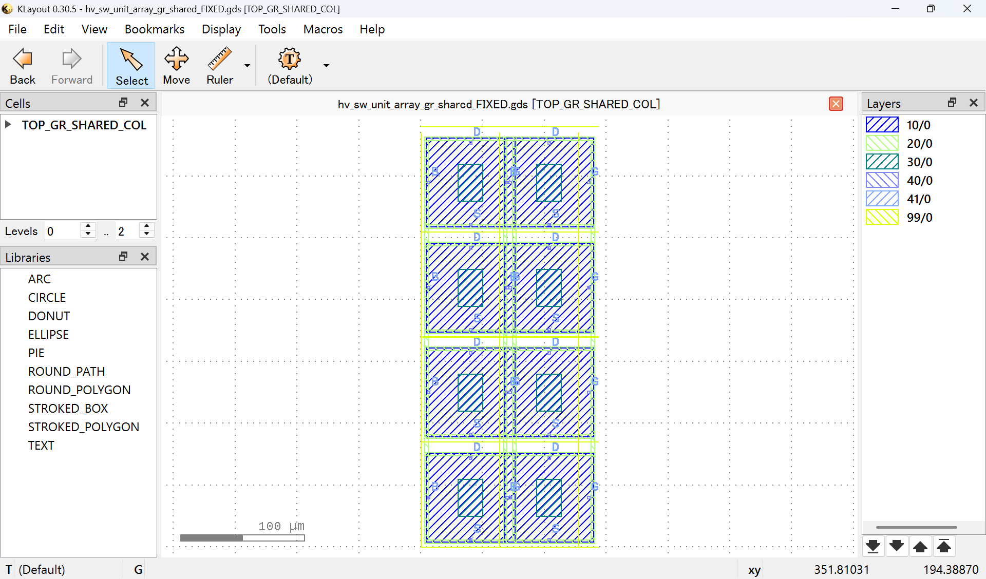
Result:
- Guard ring overlap is reduced
- But the pitch remains fundamentally too tight
Step 3: Guard-Ring-Clean (Final Check)
Finally:
- All internal guard rings are removed
- Guard rings are placed only around the array perimeter
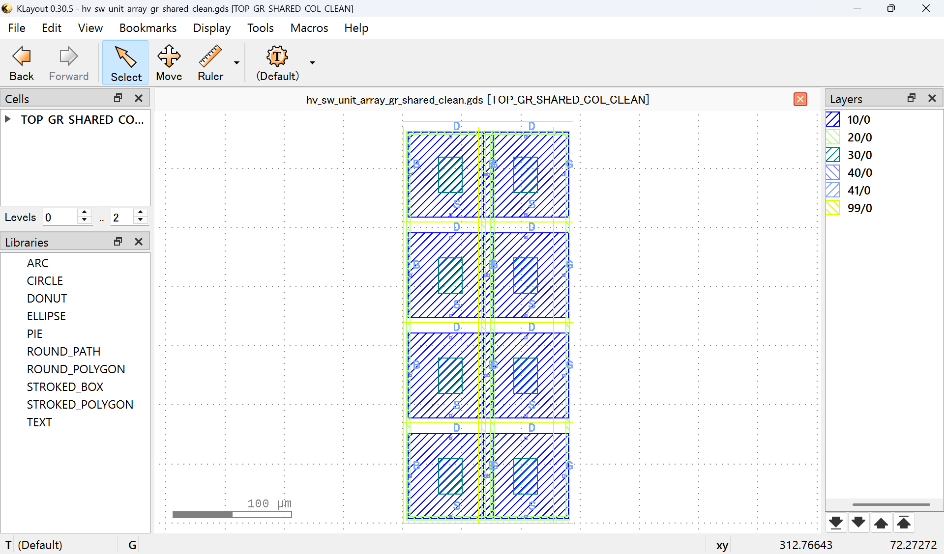
This reveals the key fact:
The ultimate limiting factor is DNWELL, not the guard ring
Note
Although the three figures appear nearly identical at first glance,
the differences lie in guard-ring placement and DNWELL dominance.
This comparison is not about drastic shape changes, but about
isolating which structure fundamentally constrains array pitch.
🚫 Conclusion: 400 dpi Is Structurally Infeasible in GF180
From the three-step evaluation, the conclusion is unambiguous:
- No matter how aggressively guard rings are reduced
- No matter how placement is optimized
DNWELL enclosure and isolation rules cannot fit within a 63.5 µm pitch
In other words:
With GF180MCU and DNWELL-based isolation,
a 400 dpi inkjet driver is structurally infeasible
This is not an assumption —
it is a design decision backed by GDS-level evidence.
✅ What About 300 dpi?
At 300 dpi, the pitch is approximately 84.7 µm.
This is clearly larger than the PoC HV_SW_UNIT width:
- HV_SW_UNIT width: ~80 µm
In fact, in the array-generation code, the change is trivial:
pitch_x = um(84.7, layout.dbu) # 25.4mm / 300dpi
Under this condition:
- DNWELL margins become physically manageable
- Unlike 400 dpi, design adjustments can plausibly close
This places 300 dpi in a realistic design region.
🛠 Next Steps at 300 dpi
Once a 300 dpi layout is physically viable, the next phase includes:
- DRC
- Full compliance with GF180 PDK rules
- PEX
- Extraction of parasitic R/C
- SPICE
- Id–Vd / Id–Vg sanity checks
- Switching transient verification
- Pad / ESD / HV routing design
From here on, the work shifts from “placement feasibility” to
IC-level completion and validation.
🧾 Summary
- 400 dpi is
physically infeasible with GF180MCU + DNWELL - 300 dpi is
realistic and worth pursuing - This study is
a layout-driven exploration with GDS-backed evidence
Most importantly:
Feasibility was judged by real layout, not expectation
This itself is the core achievement of the project.
📝 Closing Remarks
When high voltage, mixed signal, and high density intersect,
design is inevitably pulled back to physical reality.
GF180MCU Open PDK provides a rare opportunity to learn this reality
in a fully transparent and reproducible way.
Proceeding further means entering
a new phase explicitly assuming 300 dpi.
This is a natural stopping point for this exploration.
🔗 Project Context
This verification and the resulting layout work are part of:
gf180-inkjet-driver
- Objective: Physical design exploration of a
high-voltage mixed-signal driver IC for inkjet printheads - Approach: Layout-driven design rather than automation
Links
-
GitHub Repository
https://github.com/Samizo-AITL/gf180-inkjet-driver -
GitHub Pages (Design Documentation)
https://samizo-aitl.github.io/gf180-inkjet-driver/ -
Design Docs (GDS / Layout-Focused)
https://samizo-aitl.github.io/gf180-inkjet-driver/docs/
Discussion and feedback are welcome via GitHub Discussions:
https://github.com/Samizo-AITL/gf180-inkjet-driver/discussions