【Inkjet】🧪 03. Why GF180MCU × OpenLane Does Not Work — Confirmed by Real-World Verification
topics: [“semiconductor”, “openlane”, “pdk”, “gf180”, “vlsi”, “mixed-signal”, “high-voltage”, “layout”]
📌 Conclusion (Up Front)
The GF180MCU Open PDK is not compatible with OpenLane (which assumes an OpenPDK-based flow),
and an automatic flow from synthesis to P&R to GDS generation does not work.
This is not speculation.
It is a conclusion confirmed through hands-on verification in a real environment.
As a direct result of this verification,
this project abandoned the automatic digital flow and transitioned to a layout-driven design approach,
centered on high-voltage MOS (HVMOS) devices.
🧭 Background
GF180MCU is published as an Open PDK suitable for:
- High-voltage devices
- Mixed-signal design
It appears well aligned with applications such as
inkjet printhead drivers, which require HV + mixed-signal circuitry.
This led to the hypothesis:
“Perhaps we can push GF180MCU through OpenLane all the way to GDS.”
To validate this, we performed direct verification in a real execution environment.
🖥 Verification Environment (Key Points)
- OS: Ubuntu (WSL)
- Flow: OpenLane v0.23
- PDK: GF180MCU Open PDK
- Objective: Verify whether GDS can be generated via a fully automatic flow
❗ What Actually Happened (Facts)
When running OpenLane,
the flow always failed at the prep stage with the following error:
couldn't read file
.../libs.tech/openlane/config.tcl
This failure was reproducible and unavoidable.
🧠 Technical Root Cause
OpenLane assumes an OpenPDK-style directory structure,
specifically requiring:
libs.tech/openlane/config.tcl
However, this structure does not exist in the GF180MCU Open PDK.
This is not a missing configuration file or a simple setup issue.
It reflects a fundamental mismatch in PDK design philosophy.
📊 Technical Comparison
| Item | Sky130 | GF180MCU |
|---|---|---|
| Official OpenLane support | ✔ | ✘ |
| OpenPDK directory structure | ✔ | ✘ |
| Automatic GDS generation | ✔ | ✘ |
| HV / mixed-signal suitability | △ | ✔ |
In short:
GF180MCU is not “unsupported” in general —
it simply does not align with OpenLane’s assumptions.
🔍 Why This Is Not a “Failure”
What this verification conclusively established:
- GF180MCU is not a PDK intended for digital auto-P&R flows
- HV / mixed-signal design assumes layout-driven methodologies
- OpenLane is a digital-centric flow built on OpenPDK assumptions
This is a critical design boundary,
and one that cannot be reliably determined from documentation alone.
Confirming it through real execution was essential.
🚧 What We Did Next (Critical)
After abandoning the automatic flow, the project moved forward by:
- Completely decoupling from OpenLane
- Adopting manual / semi-manual layout using KLayout
- Exploring GDS-level design centered on high-voltage MOS devices
As a result, we successfully generated actual GDS data
for a high-voltage MOS switch unit (HV_SW_UNIT).
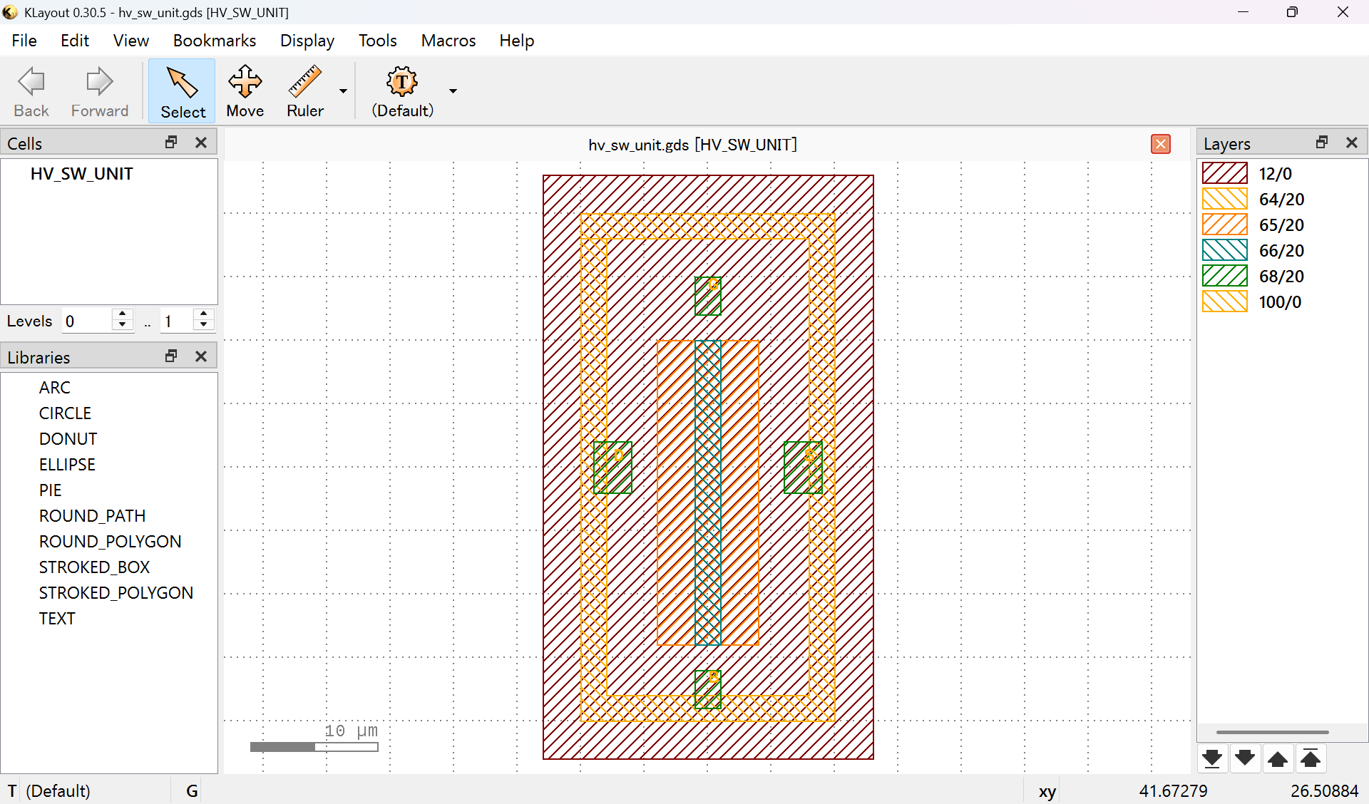
🧩 HVMOS Layout Result (Real GDS)
Below is the actual GDS generated in this project:
a GF180MCU-based high-voltage MOS switch unit (HV_SW_UNIT).
- DNWELL-based high-voltage isolation
- Continuous P+ guard ring
- Minimal HVMOS-centered switch structure
- A concrete physical interface between IC and external MEMS / actuators
At this point, the state is no longer:
“OpenLane failed to generate GDS”
but rather:
“By selecting the appropriate design methodology,
we reached real, manufacturable GDS.”
🛠 Practical Implications
When Using GF180MCU
- Manual or semi-manual layout using Magic or KLayout
- Concurrent circuit–layout thinking
- Physical design including HV spacing, wells, and guard rings
When Using OpenLane
- OpenPDK-compatible processes (e.g., Sky130)
- Digital-dominant automatic P&R flows
“HV mixed-signal × automatic digital flow” rarely intersects.
🧩 Relation to This Project
This verification and the resulting layout work are part of the following exploration project:
gf180-inkjet-driver
- Goal: Physical design exploration of a
high-voltage mixed-signal driver IC for inkjet printheads - Approach: Layout-driven design rather than automation
🔗 Links
-
GitHub Repository
https://github.com/Samizo-AITL/gf180-inkjet-driver -
GitHub Pages (Design Documentation)
https://samizo-aitl.github.io/gf180-inkjet-driver/ -
Design Docs (GDS / Layout-Focused)
https://samizo-aitl.github.io/gf180-inkjet-driver/docs/
🧾 Summary
GF180MCU × OpenLane does not work.
This is not a failure, but a crucial result in selecting the correct design flow.
GF180MCU is not:
- “A PDK for automation”
but rather:
- A PDK that assumes human-driven layout
And once that assumption is accepted,
this verification also shows that real HVMOS-based GDS is achievable.
📎 Final Note
Hopefully, this record will help reduce the number of designers
who lose time due to the same misunderstanding.