【Semiconductor】17. The Physical Origin of Pause Refresh Anomalies in 0.25 µm DRAM
topics: [“Semiconductor”, “DRAM”, “Failure Analysis”, “Device Physics”, “Process”]
🧭 Introduction
In the previous article,
we recorded only the phenomenology of the anomalies observed under Pause Refresh conditions
in 0.25 µm generation DRAM.
In this article, we organize
which physical behaviors those phenomena corresponded to.
To state the conclusion upfront,
this was not a phenomenon that could be summarized simply as “poor retention.”
The dominant factor was neither cell capacitance nor circuitry,
but process-induced leakage physics.
🔍 Physical Clues Indicated by the Observations
The observed facts listed in the previous part
all pointed in the same direction.
- Random single-bit failures
- Strong temperature dependence
- Partial reversibility
- Independence from layout and data patterns
The physical conditions that satisfy all of these simultaneously are limited.
- Occurring locally
- Thermally activated
- Not permanent destruction
At this point,
the dominant factor had been narrowed down to almost a single candidate.
🎯 Dominant Factor: Junction Leakage
The true nature of the Pause Refresh anomaly was
junction leakage current in the cell MOS transistors.
In particular, the dominant contribution came from
defect-assisted leakage levels located near:
- n⁺ / p⁻ junctions
- Diffusion edges
- Isolation boundaries (STI / LOCOS)
🧬 Cross-Sectional Structure Where Leakage Occurs (Reference)
Here, a cross-sectional diagram serving as the physical premise
for understanding the Pause Refresh anomaly is shown.
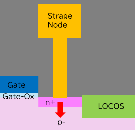
Figure 1: Junction-edge leakage paths in a 0.25 µm DRAM cell (conceptual cross-section)
What this diagram illustrates is that
leakage is concentrated not across the entire cell,
but at very localized structural edges.
- Gate edges
- Diffusion edges
- Isolation edges
All of these are locations where
process-induced damage tends to accumulate.
🔁 Behavior Governed by SRH Recombination
This leakage was governed by
Shockley–Read–Hall (SRH) recombination.
The characteristics of SRH leakage are well defined:
- Exponential increase with temperature
- Strong dependence on defect density
- Greater sensitivity to process history than to device dimensions
These characteristics naturally explain the reversible behavior whereby:
- Failures suddenly increase at high temperatures
- Failures disappear when the temperature is lowered
🎲 Why Do Failures Appear as “Random Single Bits”?
SRH leakage is not:
- Uniform across the wafer
- Identical from cell to cell
Defects are:
- Localized
- Statistical
- Reproducible, yet lacking spatial regularity
As a result:
- Failures do not form contiguous bits
- They show no row or column dependence
- No spatial “map” can be drawn
They are therefore observed as
random single-bit failures.
🚫 Cell Capacitance Was Not the Cause
This was a critical turning point.
The Pause Refresh anomaly could not be explained by:
- Insufficient capacitor capacitance
- Insufficient design margins
Even when capacitance was increased:
- Failures did not disappear at high temperature
- The failing cells remained the same
Retention time was determined by leakage,
not by capacitance.
🧪 Strong Correlation with Process History
The failure rate showed
strong correlation with specific process conditions.
Representative examples include:
- Plasma etching conditions
- Dry ashing processes
- Surface treatments after junction formation
All of these act in the direction of:
Increasing interface defect density
When process conditions were modified, failures decreased;
when reverted, failures reappeared.
This reproducibility was
decisive evidence of a physics-driven origin.
⏸ Why Did It Manifest Only Under Pause Conditions?
During normal operation or regular refresh:
- Writing
- Reading
- Periodic recharging
make leakage difficult to observe.
Under Pause Refresh conditions:
- No charge is replenished
- Only time passes
As a result:
Leakage current × no-replenishment time
directly manifests as data loss.
Pause Refresh was therefore
a condition that exposed leakage physics directly.
🧾 Summary (Physics)
The Pause Refresh anomaly in 0.25 µm DRAM was:
- Not a design problem
- Not a capacitance problem
It was leakage physics created by process-induced defects.
- Dominant factor: SRH leakage
- Sensitivity factor: defect density
- Amplification factor: temperature
- Manifestation condition: Pause (no replenishment time)
From the outset,
this phenomenon was never something to be debated at the design level.
🔗 Primary Sources (References)
-
Legacy Technology Archive
https://samizo-aitl.github.io/Edusemi-Plus/archive/legacy/ -
0.25 µm DRAM Cases
https://samizo-aitl.github.io/Edusemi-Plus/archive/legacy/dram_025um/ -
Pause Refresh Fail Details
https://samizo-aitl.github.io/Edusemi-Plus/archive/legacy/dram_025um/pause/
⏭ Next
From the next article onward,
we will move on to the PSRAM (2001) case.
First, we will address only
what PSRAM was intended to achieve
—its structure and assumptions.