【Semiconductor】16. Pause Refresh Anomalies Observed in 0.25 µm DRAM
topics: [“Semiconductor”, “DRAM”, “Failure Analysis”, “Reliability”, “Process”]
🧭 Introduction — An Anomaly Beyond Conventional Reasoning
In the 0.25 µm generation of DRAM,
an anomaly that could not be explained by conventional empirical rules was observed.
This anomaly was known as Pause Refresh Fail.
In this article, we record—without adding interpretation—
- under what conditions it occurred,
- how it manifested in behavior, and
- how it was observed.
The causes and physical explanations are deferred to the next article.
Here, the scope is strictly limited to the phenomenon itself.
🧪 What Is the Pause Refresh Test?
The Pause Refresh test is designed to isolate and evaluate
only the retention characteristics of DRAM cells.
The basic procedure is as follows:
- 📝 Write known data into the cells
- ⏸ Stop refresh operations
- ⏳ Leave the cells completely idle for a fixed period
- 🔍 Read out the data and capture bit errors
With no access and no refresh activity,
this test observes which cells can retain charge, and for how long.
At the time, this was not a special evaluation,
but one of the standard reliability test items.
🔍 Observed Anomalies
① A Fail Bit Map That Could Not Be “Drawn”
The first strong sense of inconsistency appeared
in the distribution of the fail bit map.
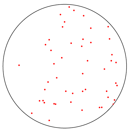
Figure 1: Fail bit map obtained under Pause Refresh conditions (0.25 µm generation DRAM)
The observed characteristics were as follows:
- No bias in the row direction
- No bias in the column direction
- No concentration at the block level
Failures appeared as
randomly scattered, isolated single-bit errors.
No “map” could be drawn along specific word lines, regions,
or wiring directions.
This behavior was clearly different
from conventional layout-related or wiring-related failures.
② Dominance of Single-Bit Failures
The majority of Pause Refresh failures were observed as:
- Not contiguous bits
- Not clustered
but as isolated single-bit errors.
There was no simultaneous multi-bit collapse,
nor failure behavior proportional to area.
At the cell level,
the failures appeared isolated and independent.
③ Extreme Temperature Dependence
When temperature conditions were varied,
the number of failures changed nonlinearly.
- 🌡 Near room temperature: almost no failures observed
- 🔥 At high temperatures: failures increased резко
Conversely, when the temperature was lowered,
some cells recovered and no longer failed.
This reversibility differed fundamentally
from permanent defects or mechanical damage.
④ No Data Pattern Dependence
Changing the written data—
- All-0
- All-1
- Checkerboard
- Random
—produced no significant difference in the number or distribution of failures.
No reproducible dependence on data content
or adjacent bit states was observed.
🧱 Reference Structures for Considering Cell Correlation
At this stage, the root cause was still undetermined,
but as a prerequisite for discussion,
the spatial relationships of the cell structure were shared.
Memory Cell Planar Layout (Reference)
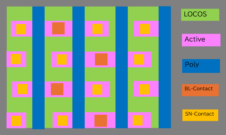
Figure 2: DRAM memory cell planar layout (conceptual)
Memory Cell Cross-Section (Reference)
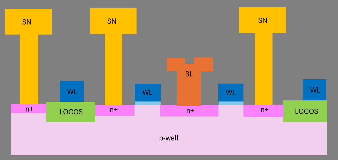
Figure 3: DRAM memory cell cross-sectional structure (conceptual)
What mattered was that
no direct cause could be inferred from these diagrams.
- No linkage to specific structures
- No directional dependence
- No layout dependence
The randomness of the fail bit map
did not correspond one-to-one with the cell structure.
✅ Facts Established at This Stage
From the observed results,
the following points were shared relatively early:
- No indication of insufficient cell capacitance
- Not a layout- or wiring-induced failure
- Not a failure occurring during access operations
Pause Refresh Fail existed conclusively only as:
Charge loss occurring in random cells during retention
—nothing more, nothing less.
⚠️ What the “Inconsistency” Suggested
This anomaly simultaneously exhibited:
- Reproducibility
- Strong dependence on conditions (especially temperature)
- Yet no spatial regularity
At this stage,
- Naming the failure mechanism
- Hypothesizing the cause
were both still inappropriate.
The only certainty was that
it did not match conventional DRAM failure models.
🧾 Summary (Phenomenology)
The Pause Refresh anomaly observed in 0.25 µm DRAM
had the following characteristics:
- Appeared only under Pause Refresh conditions
- Failures were random single-bit errors
- Strong temperature dependence with partial reversibility
- No data or layout dependence
Only the sense of inconsistency came first.
That inconsistency would later
push the discussion into
an entirely different physical domain.
🔗 Primary Sources (References)
-
Legacy Technology Archive
https://samizo-aitl.github.io/Edusemi-Plus/archive/legacy/ -
0.25 µm DRAM Cases
https://samizo-aitl.github.io/Edusemi-Plus/archive/legacy/dram_025um/ -
Pause Refresh Fail Details
https://samizo-aitl.github.io/Edusemi-Plus/archive/legacy/dram_025um/pause/
⏭ Next
In the next article,
we will address which physical behaviors this phenomenon corresponded to.
Interpretation will be provided,
but we will not step into design discussions.