【Semiconductor】⚡ 08-09. What Is HCI? — Why High Electric Fields Destroy MOSFETs
topics: [“Semiconductor”, “HCI”, “Reliability”, “MOSFET”, “BSIM4”]
⚡ Introduction
In the previous article, we discussed
NBTI (Negative Bias Temperature Instability),
a reliability degradation mechanism dominated by time and temperature.
In this article, we focus on another major degradation mechanism:
👉 HCI (Hot Carrier Injection).
- NBTI: ⏱️ Time × Temperature
- HCI: ⚡ Electric Field × Energy
In other words, HCI represents:
“The price paid for pushing a device to operate faster and harder.”
🔥 What Is HCI?
HCI is a reliability degradation phenomenon that occurs in MOSFETs when:
- A high drain voltage is applied
- A strong electric field forms near the drain
- Carriers gain very high kinetic energy (hot carriers)
Key characteristics include:
- HCI appears predominantly in nMOSFETs
- It is accelerated under high-speed and high-voltage operation
This clearly distinguishes HCI from NBTI.
🧠 What Is Happening Physically?
Near the drain region, MOSFETs experience:
- A steep potential gradient
- Extremely strong lateral electric fields
As a result:
- Carriers are strongly accelerated
- They reach high-energy (hot carrier) states
- Some carriers are injected into the gate oxide
- Interface states and oxide traps are generated
👉 The MOSFET damages its own gate oxide.
This is the essence of HCI.
📉 Impact on Device Characteristics
HCI-induced damage manifests as:
- Threshold voltage variation
- Carrier mobility degradation
- Reduced drain current
- Degraded output characteristics (Vd–Id)
Most importantly, these effects are observed as:
Changes in DC characteristics after prolonged high-$V_d$ operation
🆚 Difference Between NBTI and HCI
| Aspect | NBTI | HCI |
|---|---|---|
| Primary device | pMOS | nMOS |
| Dominant factor | Time, temperature | Electric field, voltage |
| Damage location | Interface states | Interface + oxide |
| Main effect | $V_t$ shift | Mobility loss, $I_d$ reduction |
| Dependence | Time-dependent | Voltage / field-dependent |
👉 They are fundamentally different degradation mechanisms
👉 Their mitigation strategies are also different
📐 How BSIM4 Treats HCI
In BSIM4, HCI is represented by:
- Modeling degradation as parameter variations
- Assuming degradation depends on electric field and bias conditions
- Comparing device characteristics before and after degradation
However, an important limitation must be noted:
BSIM4 alone does not directly simulate time evolution
Therefore, SemiDevKit adopts a hybrid approach:
- 🧪 SPICE: Accurate extraction at $t = 0$
- 🧮 Python: Time-dependent degradation modeling for $t > 0$
🧰 HCI Analysis with SemiDevKit
The following module is used:
- BSIM4 Analyzer Reliability
https://samizo-aitl.github.io/SemiDevKit/bsim/bsim4_analyzer_reliability/
This framework provides fully automated:
- Initial Vg–Id / Vd–Id extraction
- Threshold voltage extraction using gmmax and constant-current methods
- Application of HCI degradation models
- Reconstruction of degraded device characteristics
🔬 HCI Analysis Flow
t = 0
 ├─ VG–ID sweep
 │     ├→ Vtg0 (gmmax method)
 │     └→ Vtc0 (constant-current method)
 ├─ DC extraction
 │     └→ Idlin0 / Idsat0

t > 0
 ├─ Apply ΔVth(t) model
 ├─ Apply ΔId(t) model
 ├─ Reconstruct Vtg1 / Vtc1 / Idlin1 / Idsat1

→ Export CSV results
→ Generate degradation plots
→ Overlay VG–ID curves
🚀 Execution Example
cd bsim/bsim4_analyzer_reliability/run
python run_hci_nmos.py
📊 Example Results
■ NMOS HCI: Vg–Id Degradation (Linear Scale)
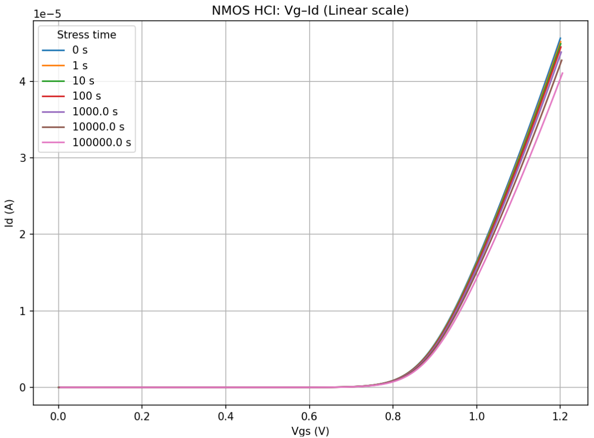
👉 Reduced $g_m$ and on-current
👉 A direct cause of critical-path delay increase
■ NMOS HCI: ΔVtg vs. Stress Time
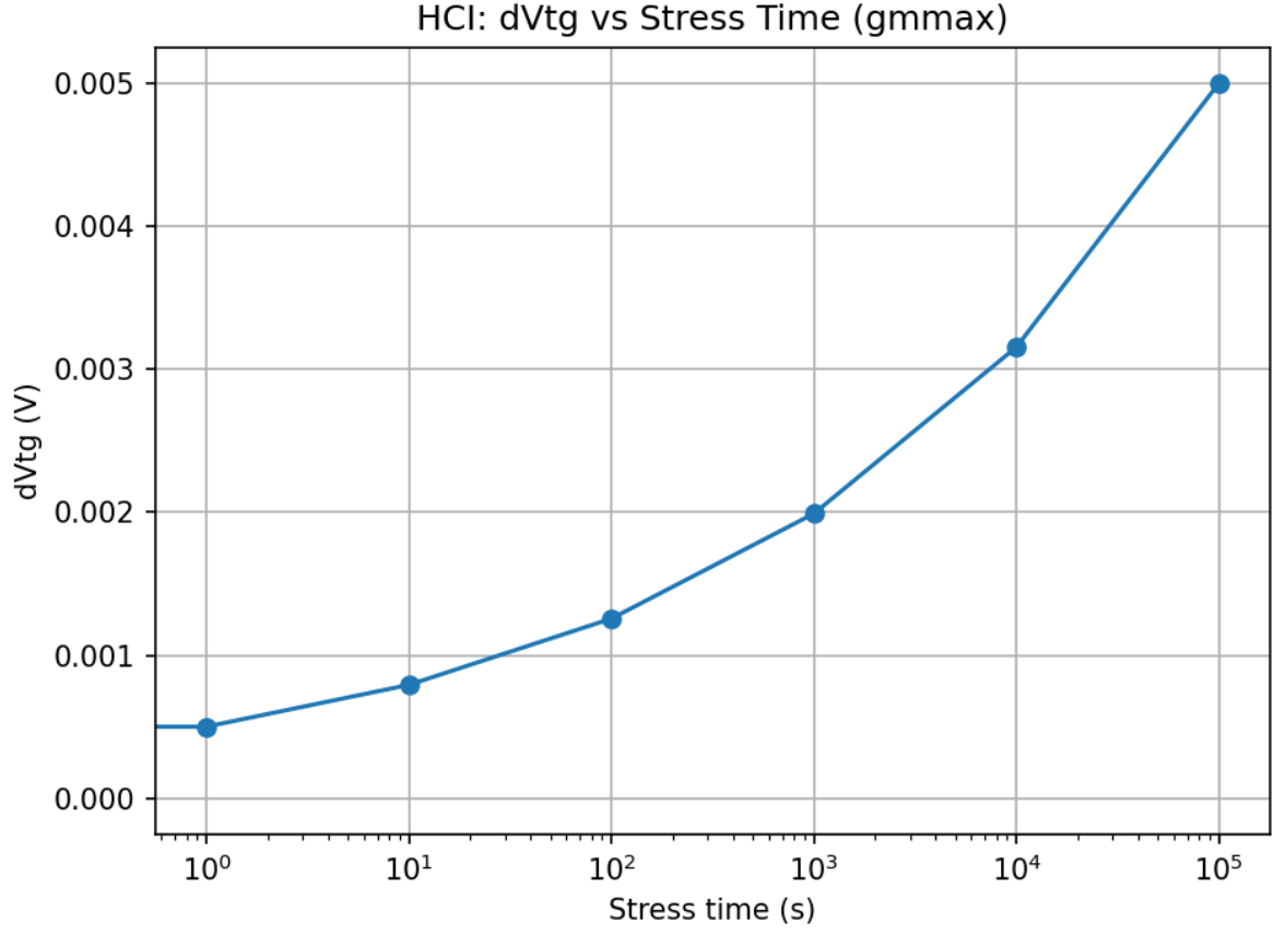
👉 Early-stage degradation dominates
👉 Higher voltage conditions accelerate degradation
⚠️ Why HCI Matters
HCI is strongly linked to:
- High-frequency clock design
- High-voltage margin design
- Output driver reliability
It clearly illustrates the trade-off:
“Chasing performance shortens device lifetime.”
🔗 TCAD / BSIM / SPICE: A Single Continuous Chain
HCI fits naturally into the same framework as previous topics:
- TCAD: High electric fields and energetic carriers near the drain
- BSIM4: Parameterized degradation modeling
- SPICE: Circuit-level impact evaluation
👉 Physics → Model → Circuit → Degradation
This single conceptual chain is completed in the HCI chapter.
📚 Series Summary
Throughout this series, we consistently followed this path:
- TCAD (physical phenomena)
- BSIM4 (compact modeling)
- Paramus (model generation)
- SPICE (DC / AC / CV analysis)
- DIM (L/W scaling)
- Reliability (NBTI / HCI)
With SemiDevKit, it is possible to experience the entire flow without relying on commercial EDA tools.
📝 Summary
- ⚡ HCI is a high-electric-field-induced degradation mechanism
- 🔵 It primarily affects nMOSFETs
- 🚀 It trades performance for long-term reliability
- 🧪 BSIM4 + SPICE + Python enable clear evaluation
MOSFETs are no longer judged by:
“How fast can they run?”
but by:
“How long can they keep running fast?”
🔗 Related Links
- SemiDevKit (Project Hub)
https://samizo-aitl.github.io/SemiDevKit/