Appendix A: Figure List
This appendix provides a complete index of all figures used in this documentation.
Each figure is listed with its purpose, verification phase, and design layer.
The intent is to clarify what each figure proves, and why similar-looking figures exist (comparison cases, internal vs. external views, or intermediate vs. final results).
A.1 Control and Verification Flow Figures
| No. | Figure | Description |
|---|---|---|
| A-01 | 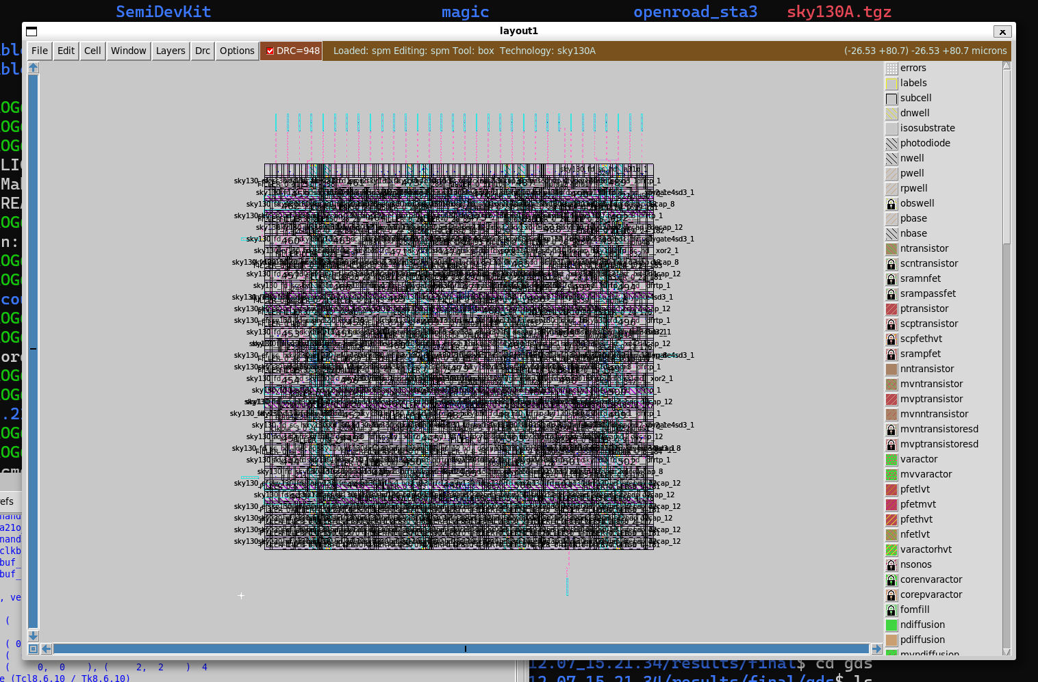 |
Standard-cell placement and routing view during the OpenLane flow. This figure is used for flow explanation and inspection, not as a final deliverable. |
| A-02 |  |
External behavior of the control logic including FSM operation. Verifies that ADC V–I inputs result in correct PWM output. |
| A-03 |  |
Internal FSM state transitions and SPI control phases. Used to validate FSM correctness and state sequencing. |
| A-04 | 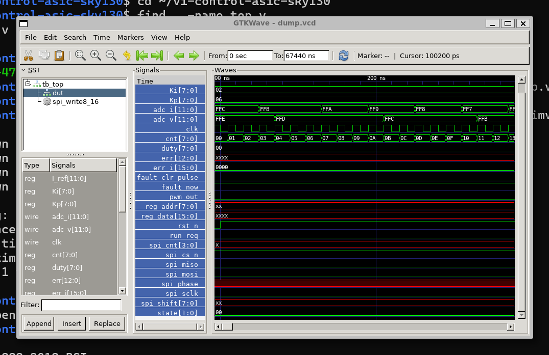 |
Functional verification of the public GitHub RTL. Confirms reproducibility and correctness of the released design. |
A.2 PID Control Arithmetic Verification
| No. | Figure | Description |
|---|---|---|
| A-05 | 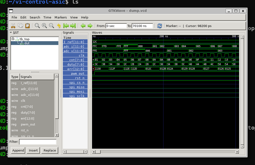 |
Step response with P-only control enabled. Verifies proportional control behavior and fixed-point arithmetic correctness. |
| A-06 | 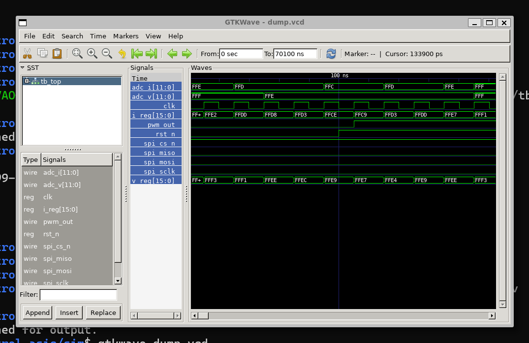 |
Step response with PI control enabled. Demonstrates elimination of steady-state error by the integral term. |
A.3 PWM to V–I Interaction Verification
| No. | Figure | Description |
|---|---|---|
| A-07 |  |
Basic relationship between PWM output and voltage/current (V–I) response. Confirms that digital PWM affects the physical model. |
| A-08 | 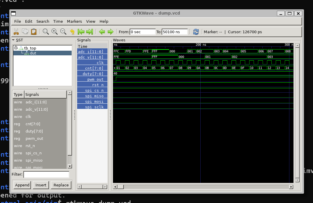 |
Comparison case with different PWM duty conditions. Verifies proportionality and repeatability of the PWM–V/I relationship. |
A.4 SPI Configuration and Integrated Verification
| No. | Figure | Description |
|---|---|---|
| A-09 | 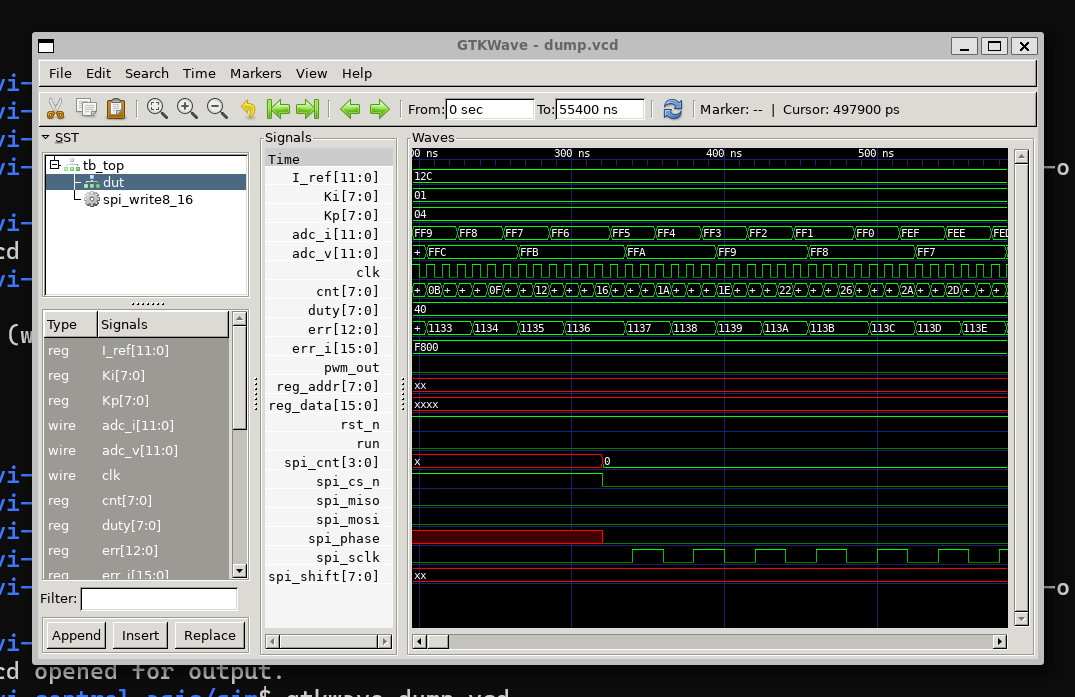 |
Verification of SPI-based configuration. Confirms that control parameters (Kp, Ki, Iref, etc.) are correctly written into internal registers. |
| A-10 | 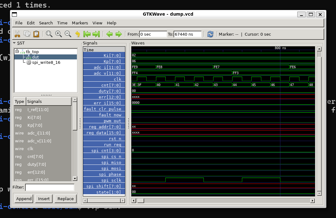 |
Integrated verification after SPI configuration. Confirms stable PI control operation without entering FAULT state. |
A.5 Physical Implementation (Final Deliverable)
| No. | Figure | Description |
|---|---|---|
| A-11 |  |
Final top-level GDS overview after completing the OpenLane RTL-to-GDS flow. This figure represents the physical implementation deliverable. |
A.6 Gate-level Simulation (Functional)
Gate-level functional simulation figures are not included in this documentation.
Although gate-level simulation was investigated after OpenLane place-and-route completion, it was determined that:
- The SKY130 standard cell libraries rely on UDP-based Verilog models
- These models are not fully supported by Icarus Verilog
- As a result, reliable gate-level functional simulation was not feasible
This is a tool limitation, not a design issue.
Functional correctness is instead ensured by:
- RTL functional simulation
- Static Timing Analysis (STA)
- DRC / LVS clean physical verification
Therefore, no waveform figures are provided for this phase.
Notes
- Figures that appear visually similar are intentionally included for:
- comparison across conditions,
- internal vs. external observation points,
- intermediate inspection vs. final results.
- This appendix serves as a figure index for reviewers and readers.
- All verification steps follow a staged and reproducible ASIC design flow.