🏭 OpenLane Flow (RTL → GDS)
This chapter explains how the RTL developed in previous chapters is transformed into a manufacturable ASIC layout (GDS) using OpenLane and SkyWater SKY130.
The focus is on understanding the flow, not just running commands.
🎯 Goal of This Chapter
By the end of this chapter, you will understand:
- What happens at each stage of the OpenLane flow
- Why each step is required
- How to interpret basic PPA (Performance / Power / Area) results
- How digital control logic maps onto physical silicon
🧰 Toolchain Overview
The OpenLane flow integrates several open-source tools:
- Yosys – RTL synthesis
- OpenROAD – Floorplanning, placement, CTS, routing
- Magic / KLayout – Layout viewing and DRC
- Netgen – LVS (Layout vs. Schematic)
All steps target the SkyWater SKY130 open PDK.
📂 OpenLane Directory Structure
A typical OpenLane design directory looks like this:
openlane/
└─ vi_control_core/
   ├─ config.tcl
   ├─ pin_order.cfg
   └─ runs/
The config.tcl file defines clock parameters,
utilization targets, and design constraints.
⚙️ Key Configuration Parameters
Important parameters in config.tcl include:
DESIGN_NAMEVERILOG_FILESCLOCK_PORTCLOCK_PERIODFP_CORE_UTIL
Example (conceptual):
set ::env(CLOCK_PORT) "clk"
set ::env(CLOCK_PERIOD) "20.0"
set ::env(FP_CORE_UTIL) 50
These values directly affect timing, area, and routability.
🧠 Step 1: Synthesis
During synthesis:
- RTL is translated into a gate-level netlist
- Flip-flops, adders, and multipliers are mapped to standard cells
Key outputs include:
- Gate count
- Estimated timing
- Area estimate
This is the first point where silicon cost becomes visible.
🧱 Step 2: Floorplanning
Floorplanning defines:
- Core area size
- Aspect ratio
- IO pin placement
- Power grid strategy
For control ASICs:
- Moderate utilization (40–60%) is recommended
- Simple rectangular layouts are usually sufficient
🧭 Step 3: Placement
During placement:
- Standard cells are placed inside the core area
- Timing-driven optimization is applied
At this stage, you can observe:
- Cell density
- Early timing slack
- Congested regions
⏱ Step 4: Clock Tree Synthesis (CTS)
CTS inserts clock buffers to ensure:
- Low skew
- Balanced clock distribution
For this design:
- Single clock domain
- No gated clocks
This simplicity greatly improves robustness and timing closure.
🛣 Step 5: Routing
Routing connects all placed cells:
- Global routing
- Detailed routing
Key checks include:
- No open or shorted nets
- Acceptable congestion
- Reasonable wire lengths
🔍 Step 6: DRC and LVS
Final sign-off checks:
DRC (Design Rule Check)
Ensures the layout follows all manufacturing rules.
LVS (Layout vs. Schematic)
Ensures the layout matches the synthesized netlist.
Passing both checks is mandatory for tapeout readiness.
📊 PPA Analysis
After completion, evaluate:
- Performance: Maximum achievable clock frequency
- Power: Estimated dynamic and leakage power
- Area: Core and die size
For educational control ASICs:
- Performance margins are usually generous
- Area is dominated by arithmetic units
- Power is modest due to low operating frequency
🧠 Educational Insight
Seeing RTL transformed into geometry is a critical learning milestone.
At this point, you should be able to:
- Point to where the PID logic resides on silicon
- Relate control complexity to chip area
- Understand timing as a physical, not abstract, property
🏁 Completion
You have now completed the full journey:
Control Theory
 → Fixed-Point Arithmetic
   → RTL Design
     → FSM & PWM
       → OpenLane
         → GDS
This is the essence of practical digital ASIC design.
🖼 Layout Inspection (OpenLane → Magic)
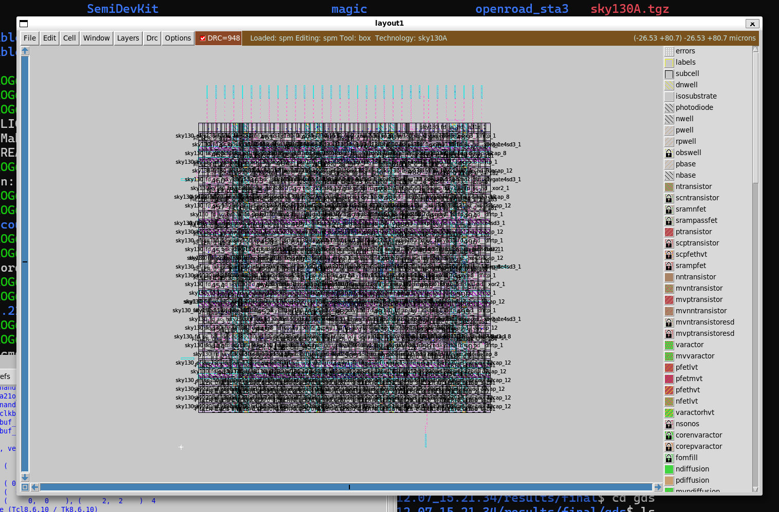
The figure above shows an intermediate placed-and-routed layout generated by OpenLane and visualized using Magic.
This view is used to inspect:
- Standard-cell placement
- Power rails
- Routing density
It is intended for flow understanding and inspection, not as the final tapeout deliverable.
📌 Next Steps (Optional)
Possible extensions include:
- Adding SPI register interfaces
- Integrating test and debug features
- Exploring alternative clock periods
- Tapeout via MPW shuttle services
🎉 Congratulations
You have reached the end of the core documentation.
If you understand every chapter in this project, you understand how to design, verify, and implement a real digital control ASIC.
➡️ Next
Proceed to post-layout verification:
➡️ Gate-level Simulation (Functional)
The next chapter verifies logical equivalence between RTL and the post-place-and-route gate netlist.