📘 Documentation – gf180-inkjet-driver
This directory contains layout- and GDS-oriented design notes for the
GF180-based inkjet printhead driver IC exploration.
These documents focus on:
- 🧱 Architecture definition
- ⚡ High-voltage device usage
- 🧭 Layout-driven mixed-signal design
with the explicit goal of supporting manual GDS generation using the
GF180MCU Open PDK.
Rather than serving as a complete IC specification, these materials function as:
- 📐 Design rationale
- 🧾 Layout justification
- 🧪 Recorded architectural limits discovered at the GDS level
Both successful structures and explicitly failed approaches are preserved, grounded in what was physically drawable and verifiable in GDS.
🔗 Links
| Language | GitHub Pages 🌐 | GitHub 💻 |
|---|---|---|
| 🇺🇸 English |
🗂 Documentation Structure
This documentation is organized by design phase and intent:
- architecture/ : frozen physical architectures
- logs/ : execution records (single source of truth)
- unit/ : HV_SW_UNIT design materials
- rules/ : process and layout constraints
- images/ : GDS screenshots and visual evidence
📒 Execution & Visual Logs (Ground Truth)
These links provide the authoritative record of what was actually executed, observed, and concluded at the GDS level.
-
🧾 RUNNING LOG — Single Source of Truth
👉 RUNNING_LOG.md -
🖼 GDS Screenshot Index
👉 GDS Images Index
🗺 Layout Map (GDS-Oriented Overview)
📌 Mermaid Rendering Note
This diagram is written in Mermaid syntax and renders correctly on GitHub.
GitHub Pages does not render Mermaid diagrams by default.👉 View the rendered diagram on GitHub:
https://github.com/Samizo-AITL/gf180-inkjet-driver/blob/main/docs/index.md
flowchart LR
  A[docs/] --> B[architecture/]
  A --> C[logs/]
  A --> D[unit/]
  A --> E[rules/]
  A --> F[images/]

  B --> B1[ARCHITECTURE.md]
  B --> B2[ARRAY_ARCH_300DPI_V1.md]
  B --> B3[ARRAY_REFERENCE_ARTIFACT_300DPI_V1.md]

  C --> C1[RUNNING_LOG.md]

  D --> D1[HV_SW_UNIT_Definition.md]
  D --> D2[HV_SW_UNIT_Floorplan.md]
  D --> D3[HV_SW_UNIT_Layout_Checklist.md]

  E --> E1[DesignRules_HV.md]
  E --> E2[HV_SW_UNIT_400dpi_Pitch_Analysis.md]
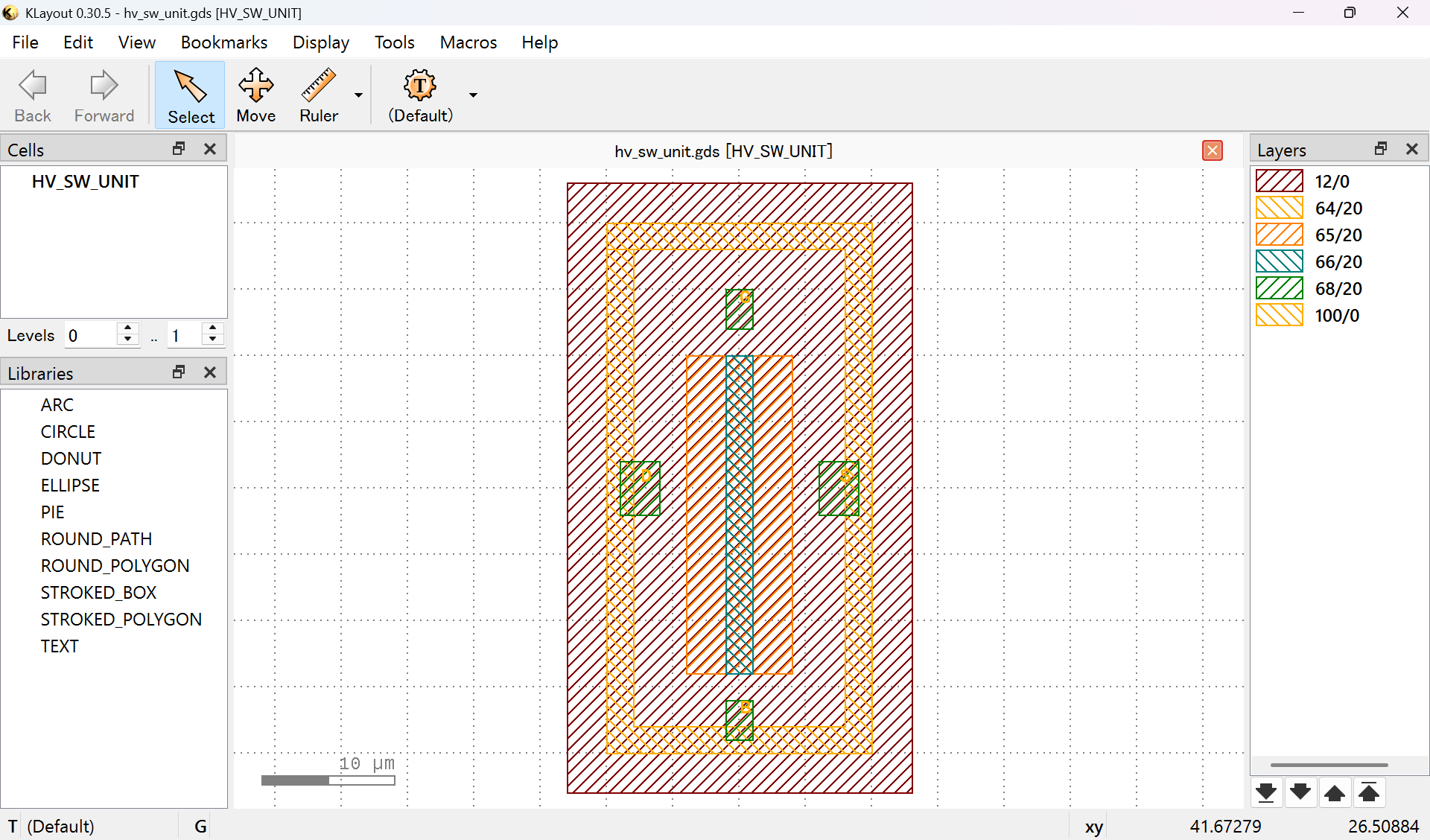
🧱 Representative GDS Artifact
The image below shows a representative HV switch unit GDS generated during this exploration.
It demonstrates:
- 🟩 DNWELL enclosure
- 🔁 Continuous P+ guard ring
- ⚡ Central HV device structure
- 📍 Explicit D / G / S / B pin exposure
🧩 Array Layout Evolution — 400 dpi Study
The following snapshots document the stepwise evolution of the HV_SW_UNIT array toward 400 dpi pitch (63.5 µm).
Each image captures a concrete layout decision and marks the point where a design assumption was validated or rejected at the GDS level.
🔹 Independent Unit Isolation (Baseline)

- DNWELL and guard ring isolated per unit
- Guard ring outer boundary dominates pitch
- ❌ 400 dpi clearly infeasible
🔹 Column-wise Guard Ring Sharing
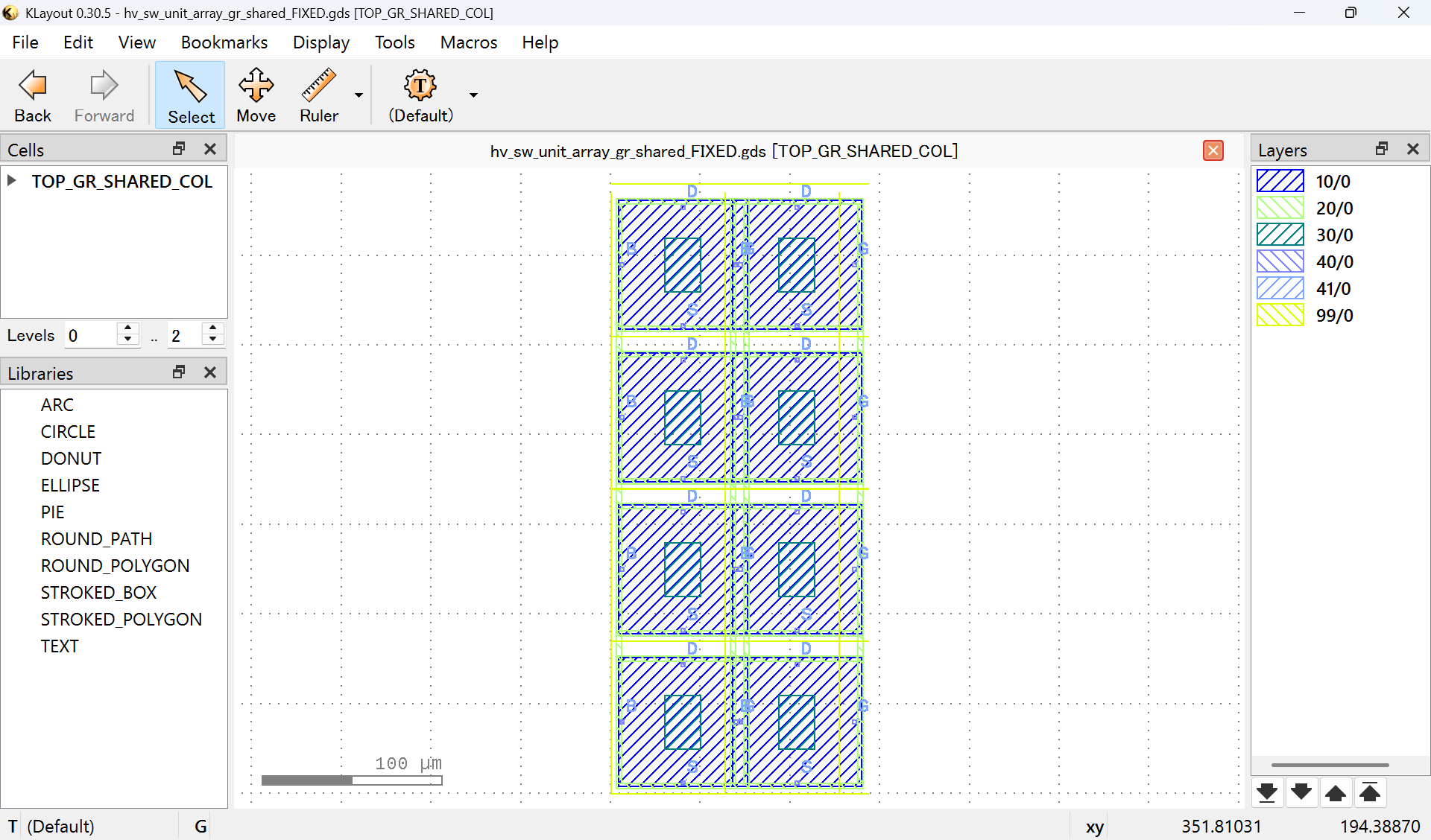
- Guard ring redundancy reduced
- Partial pitch relief achieved
- Unit-level remnants still interfere
🔹 Guard-Ring-Clean Shared Array (Final Check)
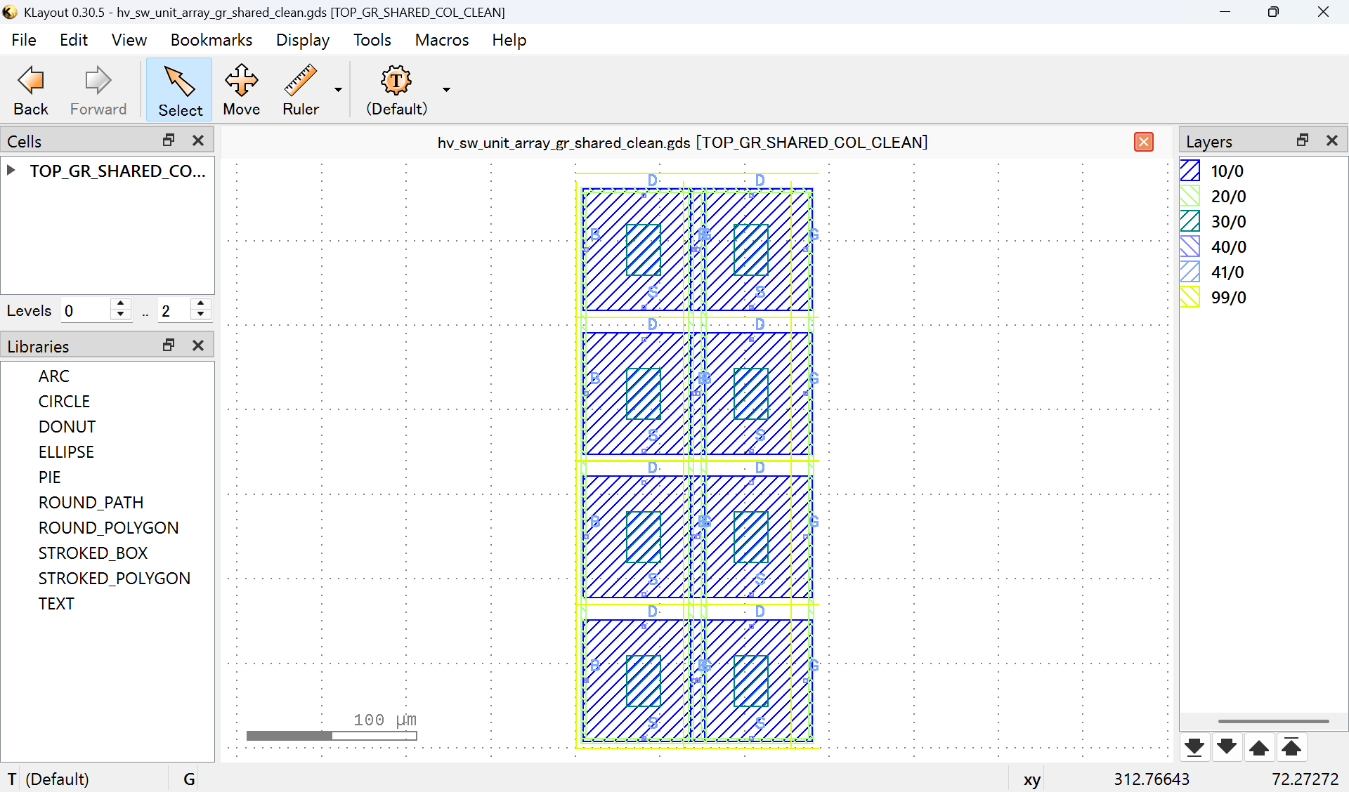
- Unit-level guard rings fully removed
- Guard ring no longer dominant
- ❌ DNWELL enclosure & spacing become decisive limiters
📚 Document Index (GDS-Oriented)
All documents are written with a clear downstream GDS target.
🧱 Architecture (Frozen)
- docs/architecture/ARCHITECTURE.md
- docs/architecture/ARRAY_ARCH_300DPI_V1.md
- docs/architecture/ARRAY_REFERENCE_ARTIFACT_300DPI_V1.md
⚡ Unit-Level Design
- docs/unit/HV_SW_UNIT_Definition.md
- docs/unit/HV_SW_UNIT_Floorplan.md
- docs/unit/HV_SW_UNIT_LW_Proposal.md
- docs/unit/HV_SW_UNIT_Layout_Checklist.md
- docs/unit/HV_SW_UNIT_IV_Expectations.md
- docs/unit/hv-devices.md
📏 Rules & Constraints
- docs/rules/DesignRules_HV.md
- docs/rules/HV_SW_UNIT_400dpi_Pitch_Analysis.md
🧠 Design Philosophy
This documentation prioritizes:
- 🧱 Layout-first decision making
- 🔬 GDS-level understanding over schematic or RTL completeness
- ✂ Minimal structures directly translatable into layout
- 📝 Explicit recording of why certain approaches fail
The goal is not a finished inkjet driver IC, but the preservation of
design reasoning grounded in physical layout reality.
📊 Status
- ✅ Automated digital flow feasibility evaluated
- ✅ Manual HV device & unit layout completed
- ✅ Array & guard-ring sharing studies completed
- ❌ 400 dpi (63.5 µm) feasibility: structurally infeasible under GF180 DNWELL rules
🧪 Why a 4×2 NMOS-Based Array Was Chosen
Before fixing 300 dpi as the baseline, a 4×2 NMOS-based HV switch array was selected as the minimum feasibility checkpoint.
Reasons:
- ⚠ Worst-case isolation first
- 🎯 Avoid edge-dominated artifacts
- 🔁 Array-level repetition & sharing check
Once 300 dpi was confirmed under this worst-case condition, it was promoted to the baseline (golden) array.
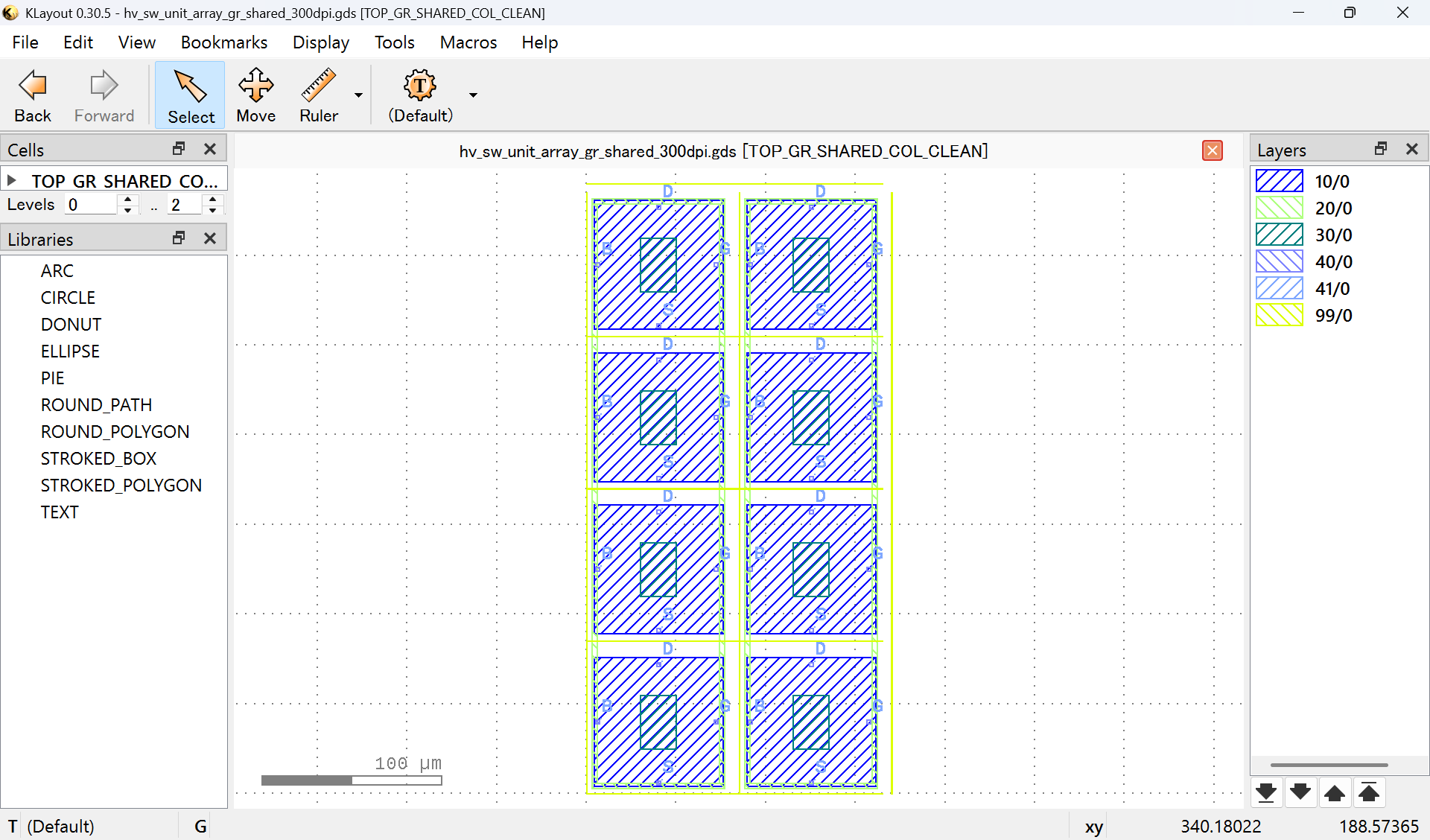
✅ 300 dpi Array — Final Outcome
A 300 dpi pitch (~85.0 µm) was selected as the minimum viable and structurally consistent solution under GF180MCU rules.
Implemented Artifact
-
🛠 Generator
layout/hv_nmos_gr/klayout/hv_sw_unit_array_gr_shared_300dpi.py -
📦 Generated GDS
layout/hv_nmos_gr/gds/hv_sw_unit_array_gr_shared_300dpi.gds -
📏 Pitch
85.0 µm (300 dpi, margin included) -
🔁 Guard Ring Strategy
Column-wise shared P+ guard ring, unit-level removed -
✅ Status
Verified in KLayout
🔌 HV Inverter 1ch Unit (300 dpi) — WIP
A 1-channel HV CMOS inverter basic cell intended for 300 dpi inkjet driver arrays.
Status: INCOMPLETE / UNDER DEFINITION
This is a physically grounded baseline, not a tapeout-ready macro.
Evidence (GDS)
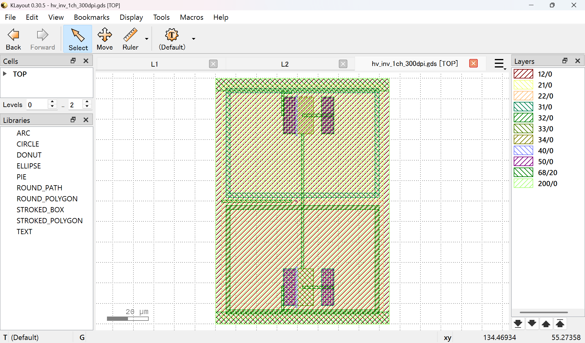
Figure — HV Inverter 1ch basic cell @300 dpi
This GDS snapshot is the single source of truth for the statements below.
Fixed Rules
- Cell center = VOUT trunk
- Horizontal tiling at 300 dpi without cumulative offset
- HV intent expressed by gate offset + drain-side drift, not cell shift
Shown Layers (Conceptual)
dnwell / nwell / pwell / n+ / p+ / poly / contact / metal1 / bbox
Known Missing (Intentional)
- Not DRC/LVS ready
- VIN routing undefined
- Guard ring & power strategy handled at top/array level
Docs
- Unit:
docs/unit/hv_inv_1ch/README.md
⚠ Disclaimer
This documentation is provided for educational and exploratory purposes only.
No guarantees are made regarding manufacturability, electrical performance, reliability, or suitability for any commercial application.