MRAM応力分布図(MRAM Stress Distribution Map)
1. 概要 / Overview
- MRAMセルにおける機械的応力は、信頼性や書き込み動作に大きな影響を与える。
Mechanical stress in MRAM cells significantly affects reliability and write performance. - 特にMTJ(Magnetic Tunnel Junction)の熱障壁低下や物理的破壊の要因となり得る。
It may reduce the energy barrier or cause physical damage to the MTJ.
2. シミュレーション設定 / Simulation Setup
- FEMソルバー:Ansys / COMSOL / Sky130版OpenFEM(仮想例でも可)
FEM solver: Ansys, COMSOL, or Sky130-compatible OpenFEM (hypothetical examples accepted). - 材料構成:MTJ層(CoFeB / MgO / CoFeB)、BE(下部電極)、TE(上部電極)
Material stack: MTJ layers (CoFeB / MgO / CoFeB), Bottom Electrode (BE), Top Electrode (TE). - 熱源:書き込みパルスによるジュール熱(Joule Heating)
Heat source: Joule heating from write pulses.
3. 応力分布結果 / Stress Map Results
- 熱-機械連成解析により、温度勾配による応力集中を確認
Thermo-mechanical coupling analysis shows stress concentration from thermal gradients. - 応力は主にMTJ中心およびCu BEとの界面に集中
Stress peaks around the MTJ and Cu-BE interface. - 以下に2次元応力マップを図示
A 2D stress distribution map is shown below.
4. 解釈と設計フィードバック / Interpretation and Design Feedback
- 応力ピークがMTJ破壊や信頼性低下と相関
Peak stress correlates with MTJ breakdown and reliability degradation. - 配線構造や層構成の最適化による緩和が有効
Stress can be mitigated through optimized interconnect and layer design.
5. SystemDK DesignKitへの反映 / Integration into SystemDK DesignKit
- BRDK/IPDKに応力耐性パラメータを追加
Add stress tolerance parameters to BRDK and IPDK. - MRAMとAMSの混載設計時に応力警告を提示するマーカー設計
Include design rule markers to warn about stress risks in MRAM-AMS integration.
6. 参考文献 / References
- [1] J. Kim et al., IEEE Trans. Electron Devices, 2023
- [2] 内製PoC構造モデルとFEM解析結果
In-house PoC structural model and FEM simulation results
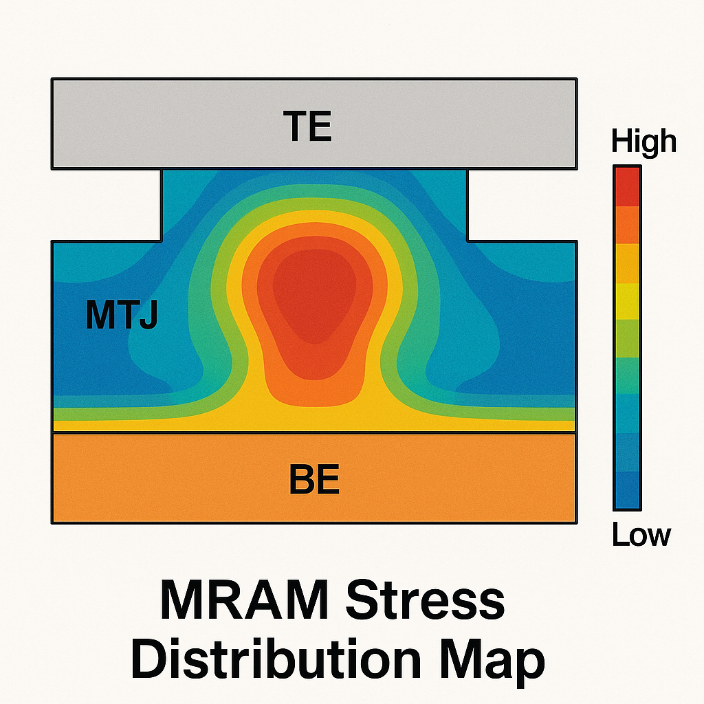
図1 / Figure 1: MRAMセル断面構造における熱-応力分布(FEMシミュレーション例)。MTJ領域において応力集中が見られる。
Simulated thermal stress distribution in an MRAM cell. Stress is concentrated around the MTJ region.