EMI制約とアイソレーション戦略(EMI Constraints and Isolation Strategy)
1. 概要 / Overview
- EMI(電磁妨害)はPoC設計において重要な設計課題である。
Electromagnetic Interference (EMI) is a critical design concern in Proof-of-Concept (PoC) development. - 特にAMS / RF回路 / MRAM / FPGA間の干渉が性能劣化の原因となる。
Interference between AMS, RF circuits, MRAM, and FPGA can degrade system performance.
2. EMI発生源 / EMI Sources in PoC Board
- PLLや高周波クロック、高dV/dtのI/Oに起因するノイズ
Noise originating from PLLs, high-frequency clocks, and high dV/dt I/Os. - MRAMの書き込みパルスによる急峻な信号遷移
Sharp transients from MRAM write pulses. - FPGAのDDRアクセスやSPI通信波形もEMI要因となる
DDR access and SPI signals from the FPGA also contribute to EMI.
3. 解析手法 / Simulation and Analysis Methods
- 近傍界 / 遠方界EMIモデリング(Near-field / Far-field)を使った評価
Evaluation using near-field and far-field EMI modeling. - PCBスタック構造と放射パターンの相関を3D EMCツールで解析
Analyze correlation between PCB stack design and radiation pattern using 3D EMC tools. - EMI-熱連成解析(例:EM波→局所発熱)も有効
EMI-thermal coupled simulation (e.g., EM wave-induced local heating) is also effective.
4. 緩和設計案 / EMI Mitigation Strategy
- GNDシールドの挿入やスタック層順序の最適化
Insert GND shielding and optimize stack-up layer order. - Power Island分割によりAMSとMRAMの電源隔離を実施
Split power islands to isolate AMS and MRAM power domains. - EMI-aware floorplanningを導入(SystemDK対応)
Apply EMI-aware floorplanning techniques (supported in SystemDK).
5. SystemDKへの制約統合 / Integration into SystemDK
- PKGDKでの伝導ノイズ・放射ノイズ制御フラグの設計
Design control flags for conducted and radiated noise in PKGDK. - EMIクリティカル領域の自動検出スクリプトと連携
Integrate with auto-detection scripts for EMI-critical regions.
6. 図解 / Figures
- EMI干渉の概念図(例:AMSとMRAM間の影響)
Conceptual diagram of EMI interference (e.g., between AMS and MRAM). - 層構造別の放射パターン例
Example radiation patterns based on different PCB stack-ups.
7. 参考文献 / References
- [1] EMI Design Guidelines for Mixed-Signal SoC, 2024.
- [2] 自作PoC構造モデルおよびEMIツール出力ログ
In-house PoC model and EMI simulation output logs.
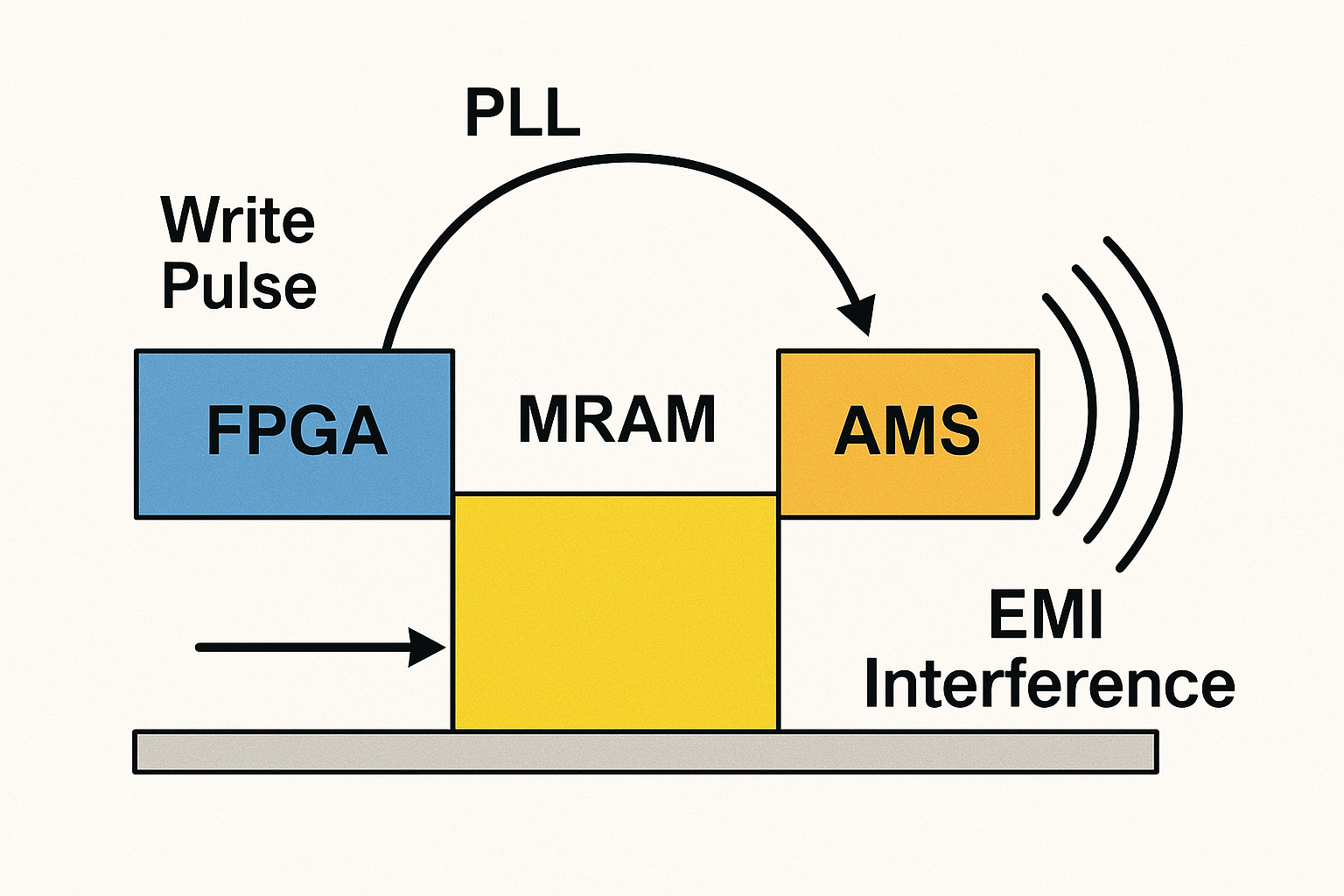
図2 / Figure 2:PoC評価ボード上のFPGA、MRAM、AMSブロック間のEMI干渉経路の概念図。書き込みパルスやPLLノイズなどがAMS回路へ影響を与える経路を示す。
A conceptual EMI interference diagram between FPGA, MRAM, and AMS blocks on a PoC board. It shows how write pulses and PLL noise affect AMS circuits.