🧪 Appendix F1_07 CFETモデル実習
Appendix F1_07: CFET Modeling Practice
🔰 概要 / Overview
本補足では、CFET構造(Stacked n/pMOS) に対応する仮想的なコンパクトモデルの実習例を提示します。
BSIM-CMG を拡張する形で「CFET版Compact Model」の概念を理解することが目的です。
This appendix provides practical exercises with a virtual compact model for CFET structures,
demonstrating how BSIM-CMG can be extended conceptually toward a future CFET-oriented model.
⚙️ 1. モデル構築の考え方 / Concept of Model Construction
- ベースモデル:BSIM-CMG(FinFET/GAA対応)
- 拡張方法:上下に nMOS / pMOS をスタックし、内部ノードで結合
- 追加パラメータ例
thermal_resistance_stack:熱結合coupling_cap_np:上下ゲート間寄生容量delay_propagation:信号遅延結合
📘 2. Spice擬似モデル例 / Example of Pseudo-Spice Model
* ===============================================
* Pseudo CFET Compact Model (Stacked nMOS/pMOS)
* ===============================================
.subckt CFET_NP_STACK D G S B
* --- Upper nMOS ---
Xn D G Nint B bsimcmg type=n fin=2
* --- Lower pMOS ---
Xp Nint G S B bsimcmg type=p fin=2
* --- Coupling elements ---
Rth Nint B  5k       ; thermal resistance (example)
Cnp G Nint  2e-15    ; coupling capacitance
.ends CFET_NP_STACK
👉 この例は 教育用の疑似定義であり、実際のBSIMライブラリには存在しません。
学習者に「モデルの拡張イメージ」を掴ませることが目的です。
🖥️ 3. シミュレーション実習 / Simulation Exercises
ここでは、擬似CFETモデルを用いた簡易的なシミュレーション実習を行います。
LTspice や ngspice で実行可能な .spice ネットリスト例を基に、熱結合や寄生容量の効果を確認します。
This section demonstrates simple simulation exercises using a pseudo-CFET model.
By running these in LTspice or ngspice, learners can observe the impact of thermal coupling and parasitics.
🧩 3.1 CMOSインバータ回路への適用 / Applying to CMOS Inverter
- nMOS/pMOS ペアを
CFET_NP_STACKに置換 - 入力電圧を掃引し、VTC(伝達特性曲線) を取得
* CFET CMOS Inverter Example
Vin in 0 DC 0
Vdd vdd 0 0.8
Xc1 vdd in out 0 CFET_NP_STACK
Xc2 out in 0 0 CFET_NP_STACK
.dc Vin 0 0.8 0.01
.plot dc V(out)
.end
Run a DC sweep on Vin to observe the inverter’s Voltage Transfer Characteristic (VTC).
🌡️ 3.2 熱結合パラメータの効果 / Effect of Thermal Coupling
Rthを変化させて、熱抵抗が小さい場合に出力特性がシフトする様子を確認- 低Rth → 熱結合が強い → 特性劣化が顕著
.param Rthval=5k
Rth Nint B {Rthval}
👉 Rthval を 1k、10k と変化させ、伝達特性の変化を比較する。
⚡ 3.3 寄生容量の影響解析 / Analyzing Parasitic Coupling
Cnpを有効/無効に切り替え、スイッチング遅延の違いを観察.tran解析で入力方形波に対する出力波形を比較
Vin in 0 PULSE(0 0.8 0ps 10ps 10ps 100ps 200ps)
.tran 0.1ps 1ns
.plot tran V(in) V(out)
👉 Cnp を 0 と 2e-15 に設定し、出力遅延の差を観察。
📊 4. 教育的効果 / Educational Value
- BSIM4 → BSIM-CMG → CFET構想 の流れを、実際に体験できる演習として理解可能
- 標準化されていないCFET領域を「仮想モデル」で試すことで、研究課題を具体的に把握できる
- 学習者が「EDAとデバイス物理の接点」を実感できる
Through these exercises, learners experience the transition from BSIM4 → BSIM-CMG → CFET models.
By working with a virtual CFET model, they gain insight into the open challenges of modeling and the
importance of EDA–device integration in future semiconductor design.
📊 5. 実行結果例 / Example Simulation Results
以下の図は 教育用の概念図 であり、実際のCFETデバイスやBSIM-CMGモデルのシミュレーション結果ではありません。
熱結合(Rth)や寄生容量(Cnp)の影響を直感的に理解するためのイメージ図として利用してください。
🔀 VTCシフト(熱結合パラメータ Rth の影響)
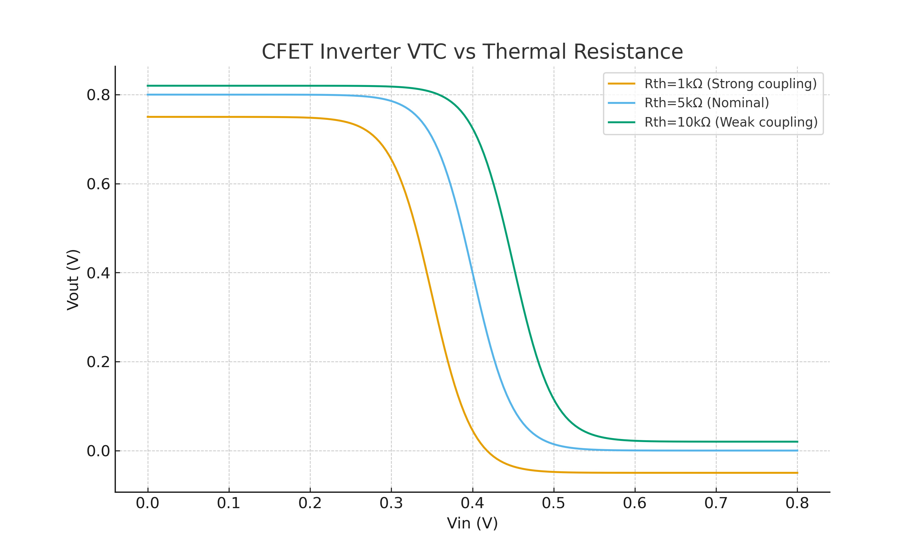
Conceptual illustration of how thermal resistance (Rth) affects the CFET inverter’s voltage transfer characteristic.
⏱️ 遅延比較(寄生容量 Cnp の影響)
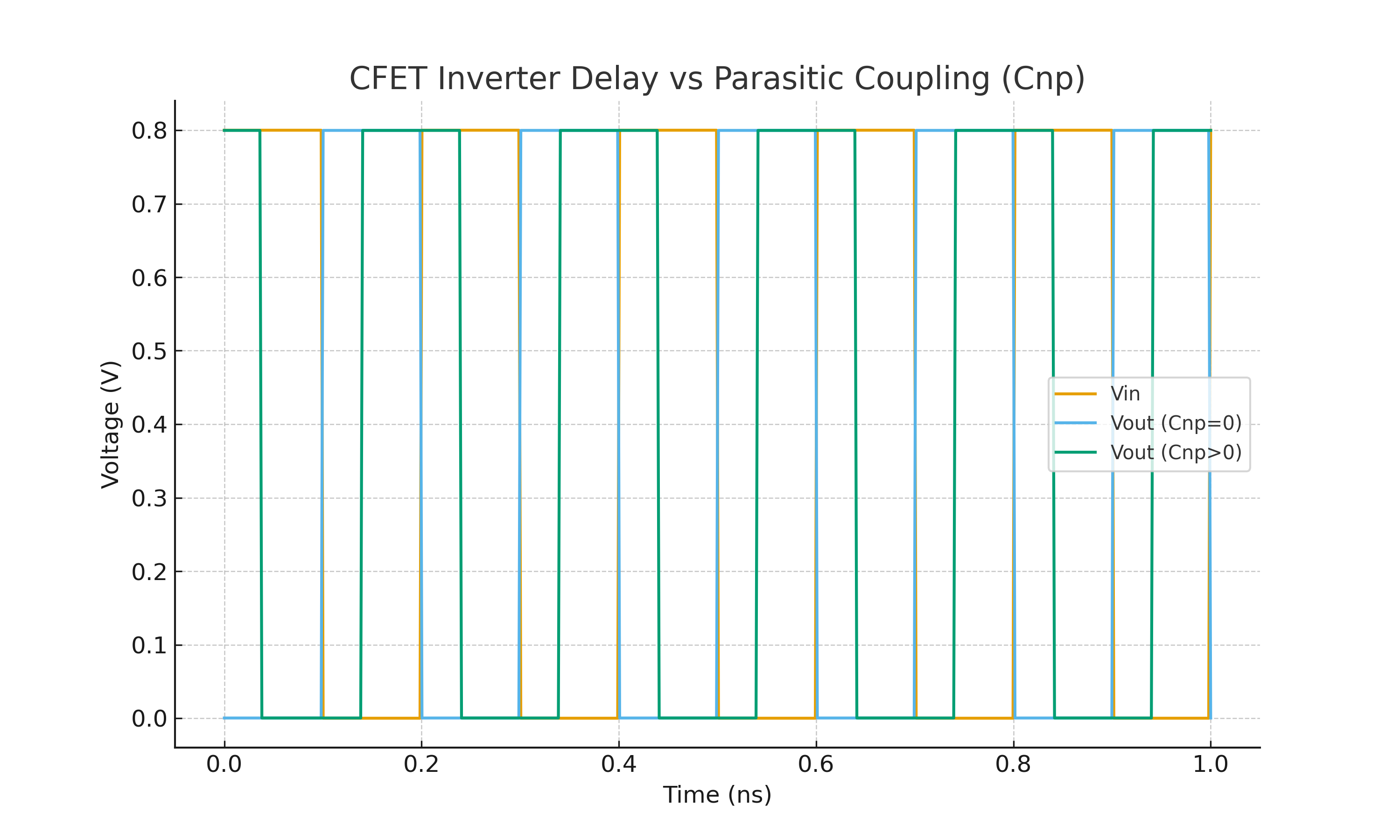
Conceptual illustration of how parasitic coupling capacitance (Cnp) impacts the delay in CFET inverter switching.