🛠 実践編 第6章: SPICE実践演習 | SPICE Practice for Devices and Circuits
本章では、Edusemi-v4x 特別編で学んだ FinFET / GAA / CFET の概念や
Wide Bandgap (SiC / GaN) の特徴を、SPICEシミュレーションで再現して確認します。
This chapter reinforces concepts from the basics through hands-on SPICE simulations.
🔗 公式リンク | Official Links
| 言語 / Language | GitHub Pages 🌐 | GitHub 💻 |
|---|---|---|
| 🇯🇵 日本語 / Japanese |
📑 演習内容 | Exercises
1️⃣ デバイス特性 | Device Characteristics
- File:
devices/nmos_iv_characteristics.spice - Run:
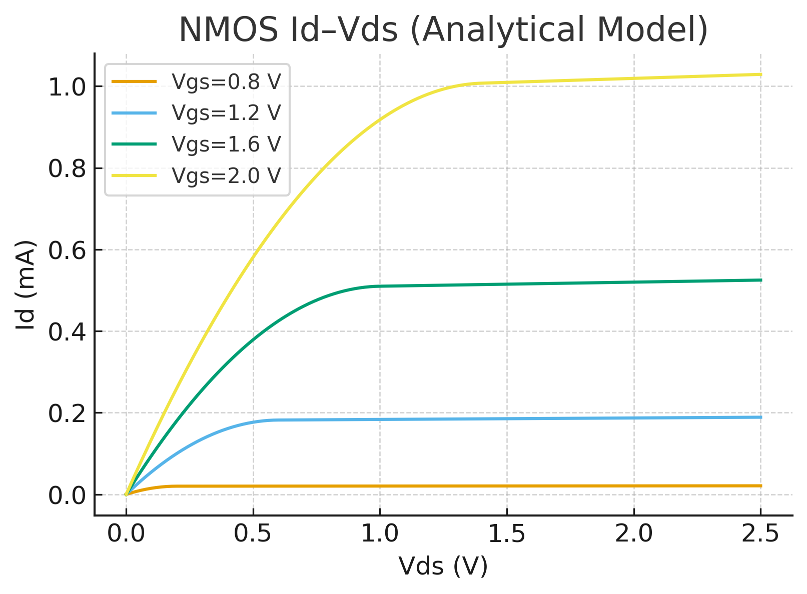
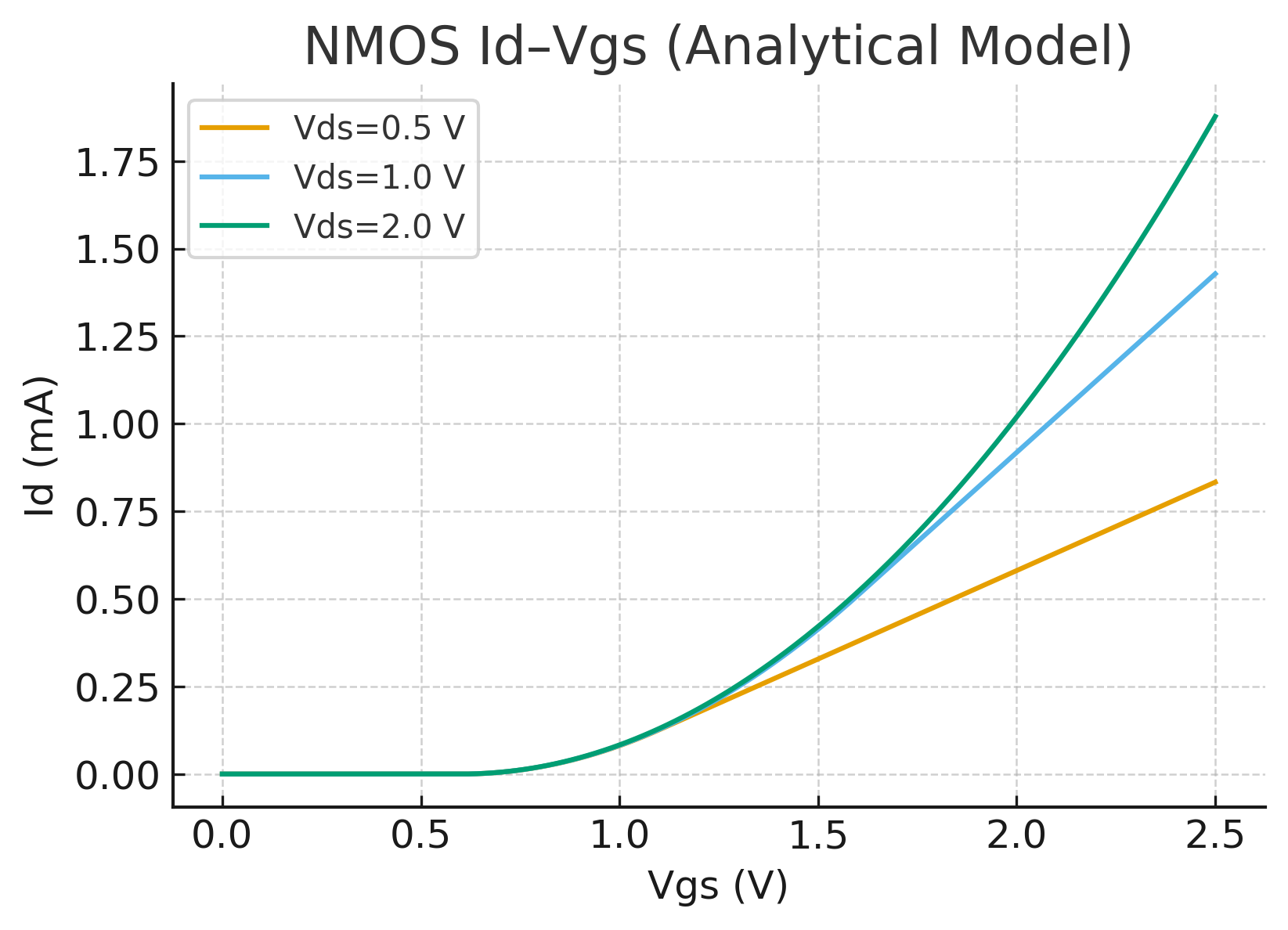
.dcで Id–Vds、Id–Vgs カーブを描画 - 学びのポイント: Vth 抽出、飽和領域・線形領域の境界
- Extract threshold voltage, observe linear vs saturation regions
2️⃣ CMOSインバータ | CMOS Inverter (FinFET vs GAA)
- Files:
circuits/inv_cmos_finfet.spicecircuits/inv_cmos_gaa.spicecircuits/inv_common_models.inc
- Run:
.tranで伝達特性(VTC)と遅延を観察 - 学びのポイント: Vth・gmの違いがノイズマージン・遅延に与える影響
- Impact of threshold voltage and gm differences on VTC and delay
3️⃣ GaN vs SiC スイッチング | GaN vs SiC Switching
- File:
power/gan_vs_sic_switching.spice - Run:
.tranで出力電圧、負荷電流、ゲート波形を比較 - 学びのポイント: 高速スイッチング (GaN) vs 高耐圧・安定性 (SiC) の違い
- Contrast fast switching of GaN vs high-voltage stability of SiC
⚙️ 前提条件 | Assumptions
- プロセスノード / Process Nodes
- Sky130 MOS → VDD=1.8 V, L=0.15 µm
- FinFET (16 nm 相当, 教材用) → VDD=0.8 V, L=15 nm, W=120 nm
- GAA (5 nm 相当, 教材用) → VDD=0.7 V, L=12 nm, W=120 nm
- SiC/GaN → VDD=400 V (Half-Bridgeスイッチング例)
- 回路条件 / Circuit Conditions
- CMOS Inverter → 負荷容量 Cload=2 fF
- NMOS DC特性 → Id–Vds (Vgs sweep), Id–Vgs (Vds sweep)
- Power Switching → 負荷 L=10 µH, R=50 mΩ, 周波数=10 MHz 相当
🖼️ 結果画像 | Results (GitHub / GitHub Pages 両対応)
NMOS Id–Vds
NMOS Id–Vgs
CMOS Inverter (FinFET vs GAA)
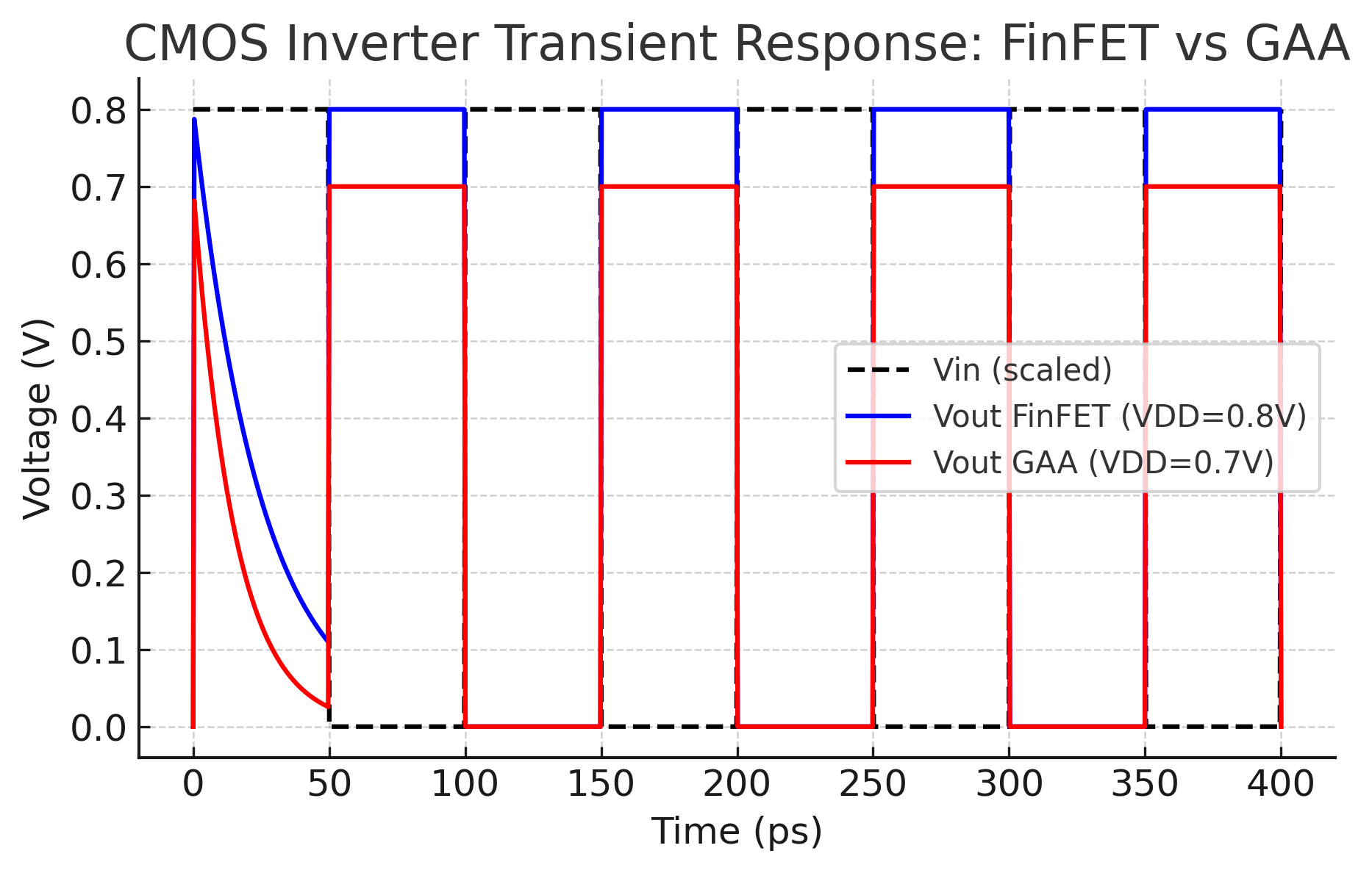
FinFET shows slower transitions, while GAA achieves faster switching due to higher gm.
➡️ inv_cmos_gaa.spice を実行
GaN vs SiC Switching
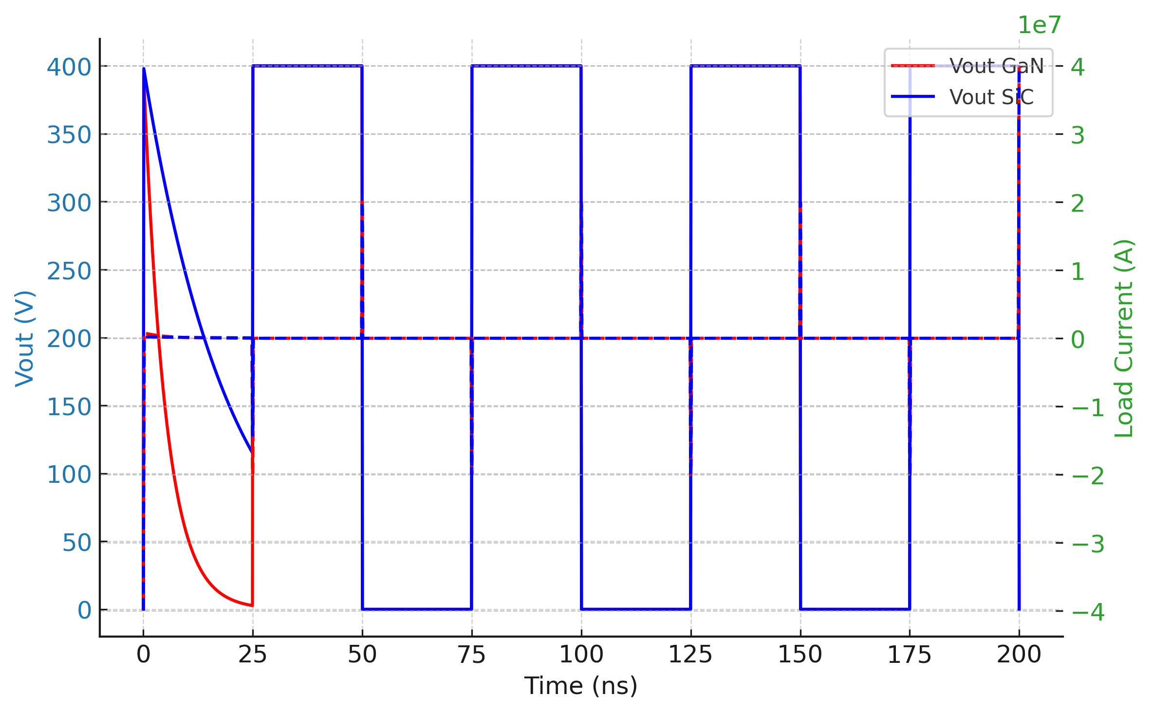
GaN shows faster switching transitions, while SiC provides more stable high-voltage handling.
➡️ gan_vs_sic_switching.spice を実行
✅ 注意事項 | Notes
- モデルは教育用の簡易パラメータ(Level=1 MOS, VSWITCH)。
- 厳密な設計には BSIM-CMG, ASM-HEMT, PDKモデル への置換が必要。
- 実行環境: NGSpice / LTspice で動作確認可能。
📘 devices/nmos_iv_characteristics.spice
* ============================================================
* NMOS Id–Vds / Id–Vgs Characteristics (Educational Example)
* Compatible: NGSpice / LTspice
* ============================================================
.option numdgt=6
.temp 25

* Bias sources
Vgs g 0 0
Vds d 0 0

* Device under test (simple Level-1 MOS for clarity)
M1 d g 0 0 NMOS_L1 L=1u W=10u

.model NMOS_L1 NMOS(Level=1 VTO=0.6 KP=150e-6 LAMBDA=0.02)

* ---- Sweep 1: Id–Vds at multiple Vgs
.dc Vds 0 2.5 0.01 sweep Vgs 0.8 2.0 0.4
.print dc V(d) I(Vds) V(g)

* ---- Sweep 2: (optional) Id–Vgs at fixed Vds
*.dc Vgs 0 2.5 0.01
*.param VDS_FIX=1.0
*Vds d 0 {VDS_FIX}
*.print dc V(g) I(Vds)

.end
📘 circuits/inv_cmos_finfet.spice
* ============================================================
* CMOS Inverter - FinFET Example
* ============================================================
.option numdgt=6
.temp 25
Vdd vdd 0 0.8
Vin in  0 PULSE(0 0.8 0 5p 5p 50p 100p)
Cload out 0 2f

M1 out in 0   0   NFIN L=15n W=120n
M2 out in vdd vdd PFIN L=15n W=120n

.model NFIN NMOS (Level=1 VTO=0.25 KP=300e-6 LAMBDA=0.05)
.model PFIN PMOS (Level=1 VTO=-0.25 KP=150e-6 LAMBDA=0.05)

.tran 1p 400p
.probe v(in) v(out)
.end
👤 著者・ライセンス | Author & License
| 📌 項目 / Item | 📄 内容 / Details |
|---|---|
| 著者 / Author | 三溝 真一(Shinichi Samizo) |
| 💻 GitHub | |
| 📜 ライセンス / License | コード / Code: MIT 教材テキスト / Text: CC BY 4.0 図表 / Figures: CC BY-NC 4.0 |
🔙 戻る|Back to Top
🏠