📘 CMOS適用限界とWBGへの分岐まとめ
Where CMOS ends and WBG (SiC / GaN / Diamond) begins
✅ 電圧・用途の棲み分け | Voltage & Application Mapping
| 技術 / Technology | 耐圧レンジ(目安) / Voltage Range | 集積度 / Integration | 主な強み / Strengths | 適用分野 / Applications |
|---|---|---|---|---|
| CMOS | 1–5 V(ロジック回路) Logic level |
⭐⭐⭐⭐⭐ 高 / High | 高集積・低消費電力 High density, low power |
CPU, GPU, DRAM, SoC |
| BCD | 5–200 V | ⭐⭐⭐ 中 / Medium | デジタル+アナログ+中耐圧を1チップ化 Mixed-signal + power integration |
PMIC, 車載IC, モータードライバ |
| LDMOS | 20–200+ V | ⭐⭐ 低 / Low | 中耐圧・高出力・RF対応 Medium voltage, high power, RF capable |
基地局PA, 車載電源 |
| SiC | 600–1200 V+ | ⭐ 低 / Low | 高耐圧・高温・高効率 High voltage, high temperature, efficiency |
EVインバータ, 産業電源 |
| GaN | 100–650 V(RF:〜100 GHz) | ⭐⭐ 低 / Low | 高速スイッチング・高周波・小型化 Fast switching, RF, compact |
充電器, サーバ電源, 5G基地局, レーダー |
| Diamond | kV〜10kV級(研究段階) | ☆ 非常に低 / Very low | 超高熱伝導・超高耐圧(理論最強) Ultra-high thermal & breakdown |
宇宙, 核融合, 将来応用 |
📊 適用領域イメージ | Application Landscape
graph TD
    A[CMOS 適用領域<br>*Low voltage, high integration*] --> B[BCD<br>*5–200 V mixed-signal power*]
    B --> C[LDMOS<br>*20–200+ V RF/PA*]
    B --> D[GaN<br>*100–650 V fast switching/RF*]
    D --> E[SiC<br>*600–1200 V high power*]
    E --> F[Diamond<br>*kV extreme future use*]
🔀 選定フロー | Selection Flow
-
SoC集積が必須?
Is SoC integration required?
→ はい → CMOS / BCD -
耐圧 > 200 V 必要?
Need >200 V blocking voltage?
→ はい → LDMOS / GaN / SiC -
> 600 V必要?
Need >600 V?
→ はい → SiC(さらにkV級なら Diamond / Ga₂O₃) -
高周波・RF用途?
RF or high-frequency application?
→ はい → GaN(特に GaN on SiC)
🎯 まとめ | Summary
- CMOSの限界 = 数十V以下、SoCやロジック領域
CMOS limit ≈ under tens of volts, for logic/SoC - 数十V〜200V → BCD / LDMOS が適用範囲
Medium voltage handled by BCD/LDMOS - 200〜650V → GaN が有利(電源小型化・RF高効率)
GaN dominates mid-voltage & RF power - 600V超 → SiC が本命
SiC leads in high-voltage & power electronics - kV級・極限環境 → Diamond(研究段階)
Diamond for extreme and future applications
🧩 System in Package 視点 | SiP Perspective
単一プロセスでは全領域をカバーできないため、実際の応用は「System in Package (SiP)」で複数チップを組み合わせるのが主流です。
Since no single process covers all domains, practical applications rely on System in Package (SiP) combining multiple dies.
🔹 役割分担 | Role Sharing
- CMOS → 制御・ロジック・インターフェース
Logic, control, interface - BCD / LDMOS → 電源管理・中耐圧駆動
Power management, medium-voltage driving - GaN / SiC → 高耐圧・高効率のパワー変換
High-voltage, high-efficiency power conversion - Diamond(将来)→ 超高耐圧・放熱の極限用途
Future: extreme high-voltage & thermal handling
🔹 実例 | Practical Examples
- 📱 スマホPMIC:CMOS制御 + BCD電源 + LDMOSスイッチ
Smartphone PMIC: CMOS logic + BCD power + LDMOS switch - 🚗 EVインバータ:SiC MOSFET + CMOSゲートドライバ
EV inverter: SiC MOSFET + CMOS gate driver - 📡 5G基地局PA:GaN HEMT + CMOS制御回路
5G base-station PA: GaN HEMT + CMOS control
🖼️ 見取り図 | Technology Integration Landscape
📊 図1: 概念モデル | Conceptual Model
CMOS = 🧠 Brain(制御・ロジック)
WBG (GaN/SiC) = 💪 Muscle(パワー・RF)
graph TB
    A[🧠 CMOS<br>*Brain: Logic & Control*]
    B[⚡ BCD/LDMOS<br>*Power Management*]
    C[💪 GaN/SiC<br>*Muscle: Power & RF*]
    D[🔮 Diamond<br>*Extreme Future*]

    A -->|Control| B
    A -->|Drive| C
    B -->|Assist| C
    C -->|High Power Domain| D
📊 図2: 技術マップ | Voltage & Application Landscape
graph TD
    A[CMOS 1–5 V] --> B[BCD 5–200 V]
    B --> C[LDMOS 20–200+ V]
    B --> D[GaN 100–650 V]
    D --> E[SiC 600–1200 V]
    E --> F[Diamond kV級]

    G["System in Package (SiP)"]
    H["Chiplet + UCIe"]

    A --> G
    B --> G
    C --> G
    D --> G
    E --> G
    F --> G
    G --> H
🖼️ 付録: 材料特性グラフ | Appendix: Material Property Charts
バンドギャップ比較 | Bandgap Comparison
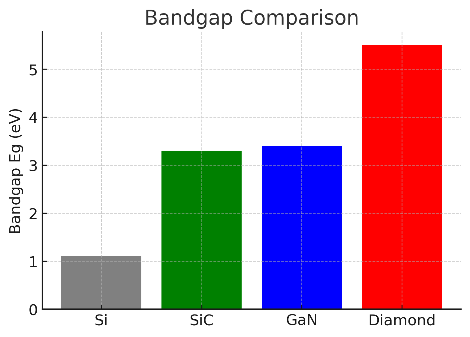
Eg values for Si, SiC, GaN, Diamond
移動度 vs Eg グラフ | Mobility vs Bandgap
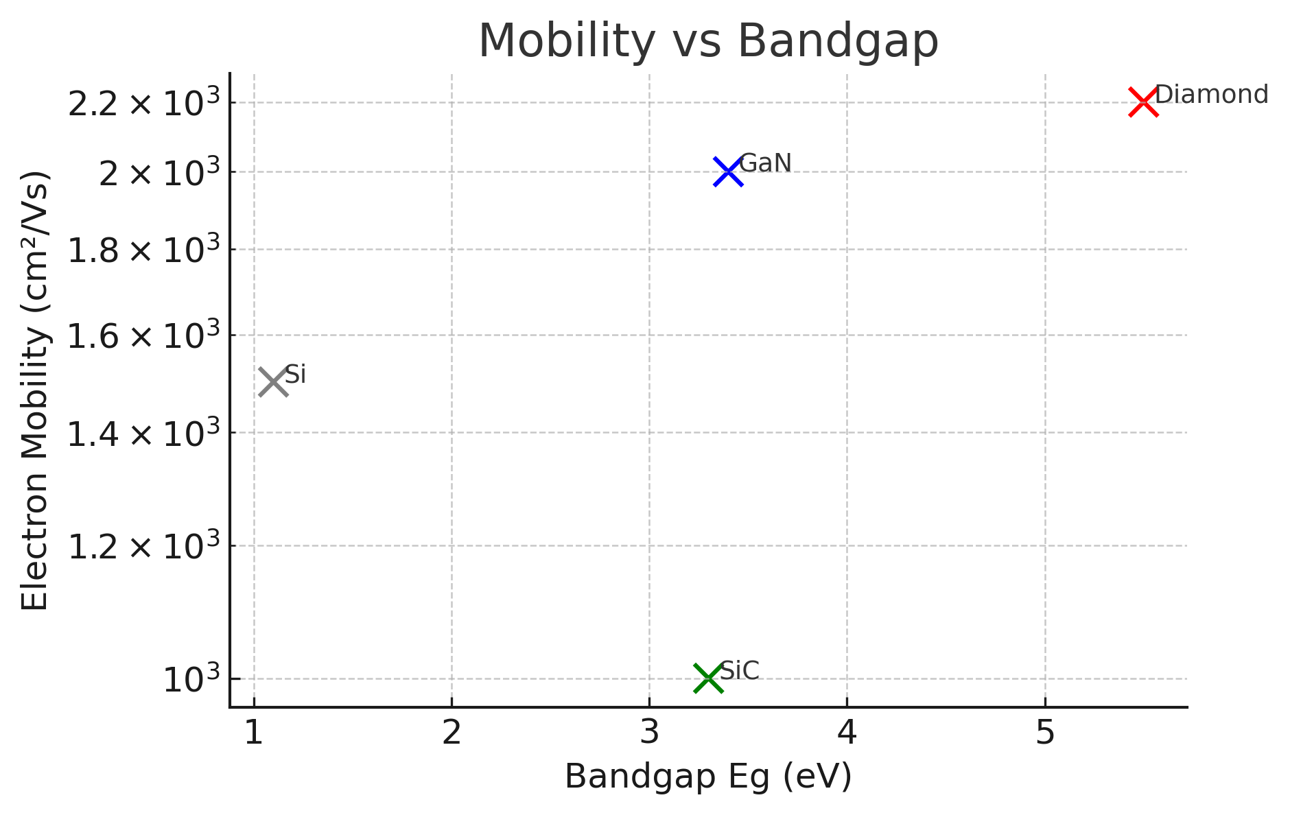
Trade-off between carrier mobility and bandgap
応用マップ | Application Mapping
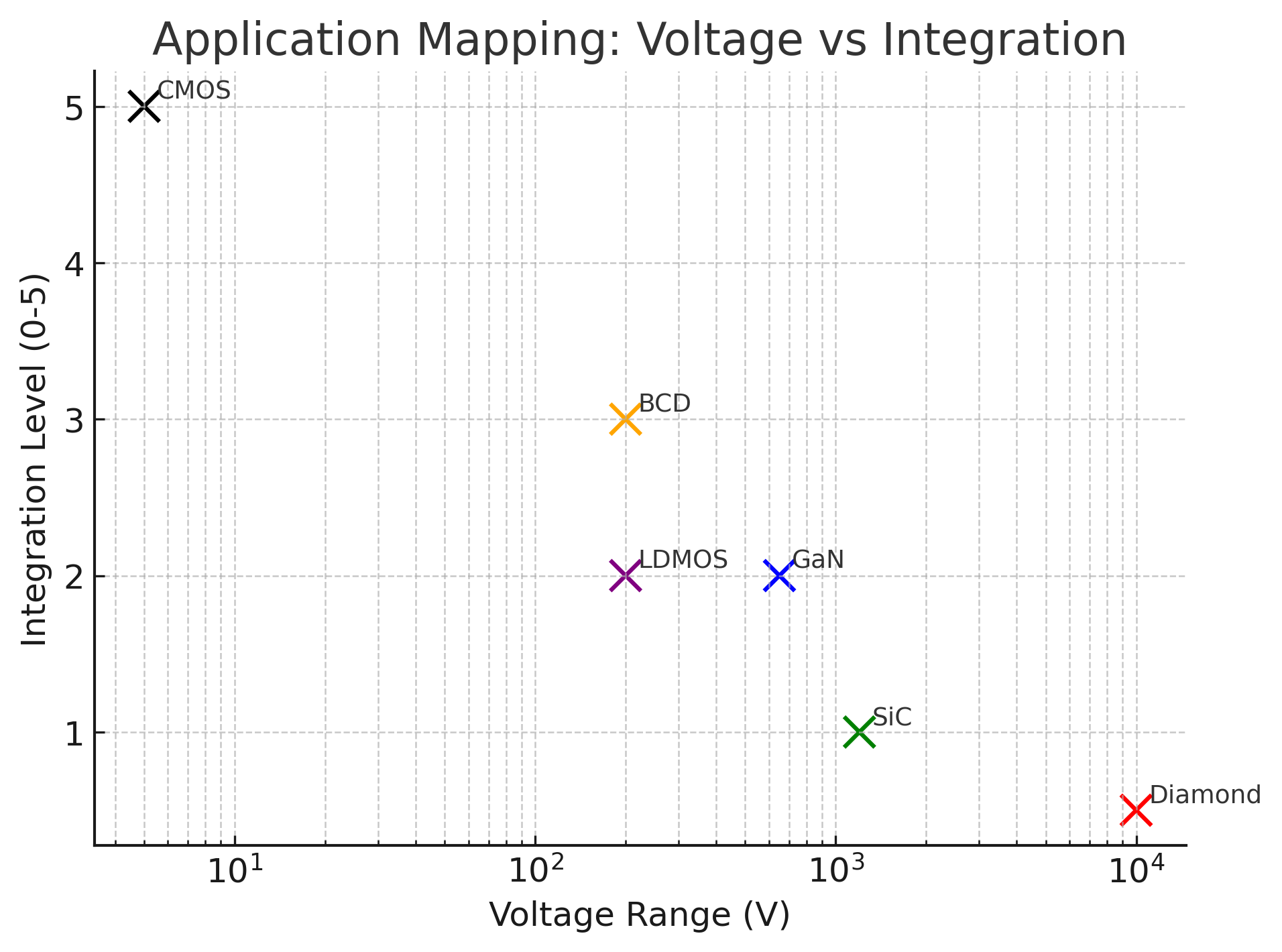
Voltage range vs Integration landscape