📊 2. 材料特性の定量比較|Quantitative Comparison of Si / SiC / GaN / Diamond
本節では、主要半導体材料 (Si, SiC, GaN, Diamond) の物理特性を定量的に比較し、
それぞれの 「強み」 と 「制約」 を明確化します。
In this section, we quantitatively compare the physical properties of Si, SiC, GaN, and Diamond,
clarifying each material’s strengths and limitations.
📌 比較視点|Key Comparison Metrics
| 項目 / Parameter | 意味 / Meaning | 重要性 / Importance |
|---|---|---|
| バンドギャップ (Eg) | 電流を流すために必要な最小エネルギー差 / Minimum energy gap for conduction | 高温特性・耐圧に影響 / Affects high-temp tolerance & breakdown voltage |
| 飽和ドリフト速度 / Saturation Drift Velocity | 電界印加時のキャリア速度限界 / Max carrier velocity under field | スイッチング速度に影響 / Impacts switching speed |
| 電子移動度 / Electron Mobility | 電界に対する電子の動きやすさ / Ease of electron movement | 抵抗・高速性に関与 / Relates to resistance & speed |
| 熱伝導率 / Thermal Conductivity | 発熱を外部へ逃がす能力 / Ability to dissipate heat | パッケージ・冷却設計に関与 / Critical for cooling & packaging |
| 絶縁破壊電界 / Breakdown Field | 絶縁破壊が起きる限界電界 / Max field before breakdown | 耐圧・小型化に直結 / Directly impacts breakdown voltage & scaling |
| 臨界オン抵抗 / Critical On-Resistance | 高耐圧FETでの理論的最小オン抵抗 / Theoretical min. on-resistance | 効率・発熱に直結 / Determines efficiency & heat loss |
📊 主要材料の物性一覧|Representative Material Properties
| 材料 / Material | Eg (eV) | 電子移動度 / Mobility (cm²/V·s) | 熱伝導率 / Thermal Conductivity (W/m·K) | 絶縁破壊電界 / Breakdown Field (MV/cm) | 臨界オン抵抗 (相対) / Critical Ron (Rel.) |
|---|---|---|---|---|---|
| Si | 1.1 | 1,500 | 150 | 0.3 | 1.0(基準 / Reference) |
| SiC | 3.3 | 900 | 490 | 3.0 | 約1/300 |
| GaN | 3.4 | 2,000 | 130 | 3.3 | 約1/400 |
| Diamond | 5.5 | 2,200 | 2,000 | 10.0+ | 約1/5000 |
💡 臨界オン抵抗は、同じ耐圧で必要とされる理論的オン抵抗の指標(Siを1とした相対値)
💡 Critical Ron is the theoretical min. on-resistance for the same breakdown voltage, normalized to Si = 1
📊 グラフ化例 | Example Graphs
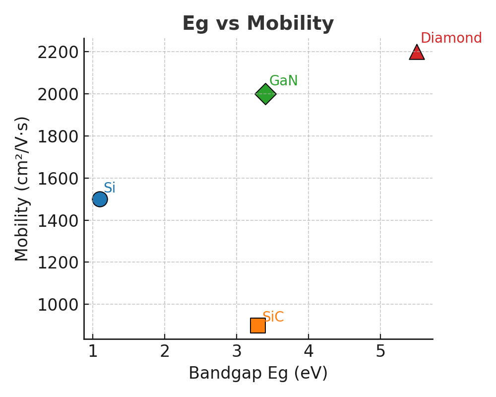
<strong>Eg と移動度の関係</strong>:WBGは一般にEgが大きいが、GaN・Diamondは高い移動度を維持。SiCは高耐圧寄りで移動度は低め。→ <strong>高周波・高速</strong>はGaN/Diamond、<strong>汎用集積</strong>はSi。<br>
<em>Relation between Eg and mobility: WBG materials have larger bandgaps, yet GaN/diamond keep high mobility; SiC is HV-oriented. ⇒ GaN/diamond for high-frequency, Si for general-purpose integration.</em>
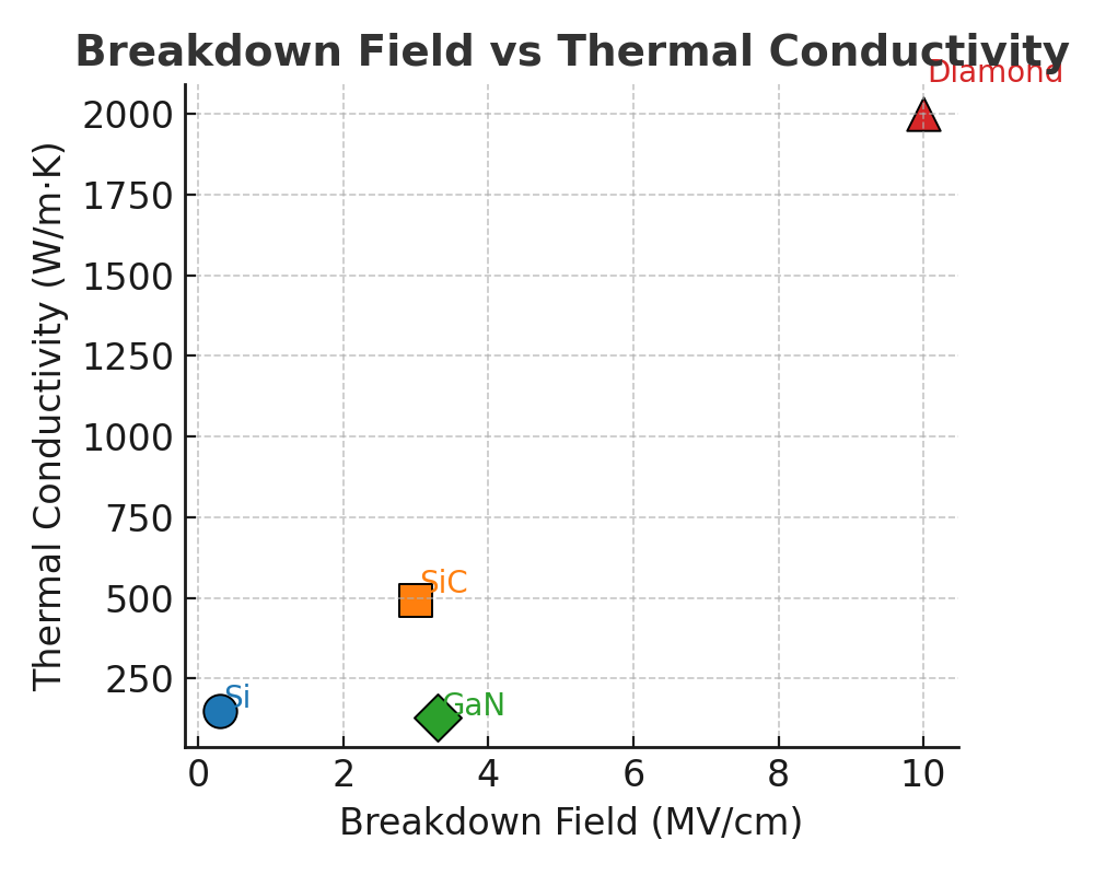
<strong>絶縁破壊電界 × 熱伝導率</strong>:SiCは両方高く<b>高耐圧・高信頼の電力</b>に最適。GaNは電界高いが熱伝導は低めで<b>放熱設計</b>が重要(GaN on SiCなど)。Diamondは理論的に突出。<br>
<em>Breakdown vs thermal conductivity: SiC scores high on both (ideal for power). GaN needs careful thermal management; diamond is outstanding in theory.</em>
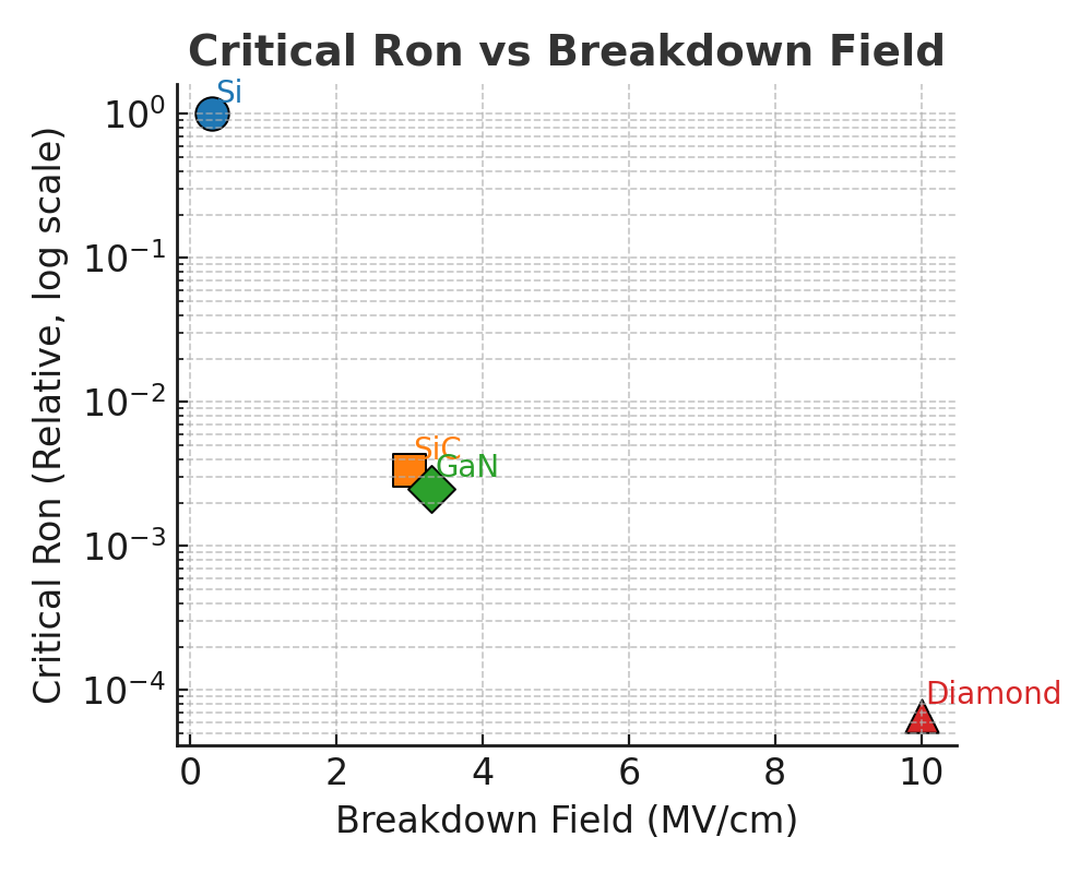
<strong>臨界オン抵抗(相対)</strong>:同耐圧ならWBGほど理論最小Ronが小さく<b>高効率スイッチング</b>が可能。SiC/GaNはSiの数百分の1、Diamondはさらに低い。<br>
<em>Critical Ron (relative): For the same breakdown, WBG enables much lower theoretical Ron → high-efficiency switching. SiC/GaN are hundreds× lower than Si; diamond lower still.</em>
🧠 材料の使いどころ|Where Each Material Excels
- Si → 標準ロジックLSI・MEMS、低耐圧・低コストが利点
Standard LSI/MEMS, low-voltage & cost advantage - SiC → 高耐圧・高温・高信頼性、EV・鉄道インバータに最適
High voltage/temp reliability, ideal for EV & railway inverters - GaN → 高速スイッチング&小型化、電源・5G・LIDARに有効
High-speed switching & miniaturization, effective for power, 5G, LiDAR - Diamond → 性能限界を超えるがコスト高、宇宙・核融合応用へ
Ultimate performance but costly, suited for space & nuclear fusion
📎 次節への接続|Next Section
3. 材料応用マッピング|Applications Mapping では、
ここで比較した材料特性が どのアプリケーションに最適化されるか を解説します。
In the next section, we discuss how these material properties map to specific applications.
🔄 ナビゲーション / Navigation
- ◀ 前節 / Previous: 1. Si・SiC・GaN・ダイヤモンド|なぜ材料を変える必要があるのか?
- ▶ 次節 / Next: 3. 材料応用マッピング|Applications Mapping
- 🔙 README: Materials|半導体材料の特性と応用選定