⏸🔁 Pause / Disturb Failures in PSRAM
This document describes how Pause and Disturb failures manifested in PSRAM, and why Disturb-related degradation became a dominant reliability concern only when the operating envelope was exceeded.
PSRAM is a representative boundary-case technology: mass-producible up to the guaranteed limit, yet rapidly exposing physical limits beyond it.
🧠 Background: PSRAM Operating Characteristics
Compared to conventional DRAM, PSRAM exhibited:
- Internally managed refresh with limited charge recovery margin
- Long effective pause time during system standby
- High-frequency access patterns during active operation
As a result, cell stress accumulated under real usage conditions, not only during explicit wafer-level test modes.
Critically, these stresses were suppressed within the guaranteed region, but became visible once temperature and usage exceeded design assumptions.
⏸ Pause Stress in PSRAM
Characteristics
- Long standby periods mapped directly to intrinsic retention stress
- Junction leakage accelerated at elevated temperature
- Residual plasma damage inherited from DRAM-era process flow
Pause stress alone weakened marginal cells, but pause-only stress did not cause failures within the guaranteed operating range.
🔁 Disturb Stress as a Dominant Failure Accelerator
Usage-Driven Disturb
In PSRAM, disturb stress accumulated during normal operation:
- Repeated word-line activation driven by application behavior
- No explicit disturb test required
- Failures emerged after resume from standby
📌 Disturb was no longer a test condition
→ it became a usage condition.
However, disturb-induced degradation remained fully suppressed until the operating envelope was exceeded.
⚛️ Device-Level Origin of Disturb Degradation
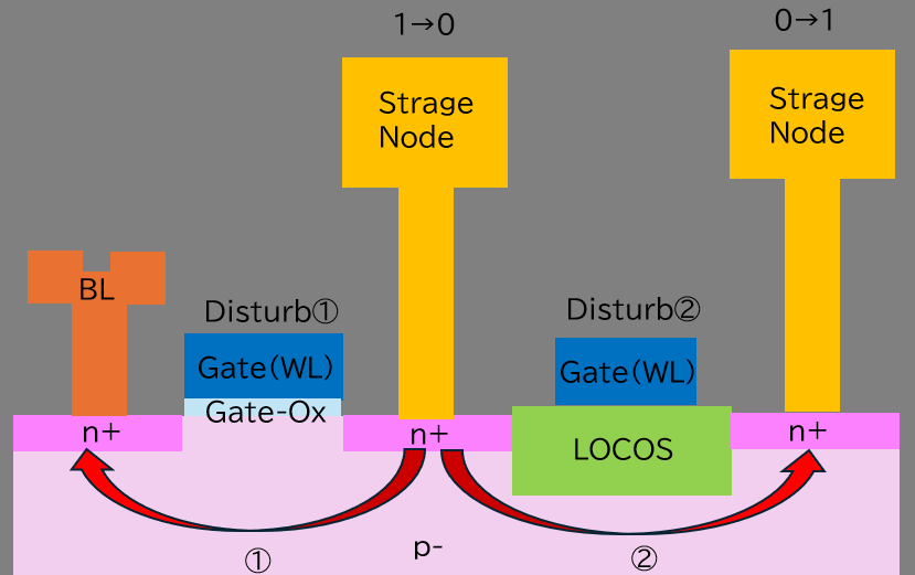
Fig. Device-level leakage paths and disturb mechanisms observed in PSRAM cell structures
Disturb stress caused:
- Increased cell transistor subthreshold leakage
- Enhanced n⁺ / p⁻ junction leakage
- Leakage across isolation regions
- Progressive charge loss from storage nodes
These effects were negligible in standard DRAM usage and remained suppressed in PSRAM up to the guaranteed region.
🌡 Temperature Expansion Impact
PSRAM required an expanded operating guarantee:
- Conventional DRAM limit: 80 °C
- PSRAM shipment guarantee: 90 °C
To ensure manufacturability and field reliability, a guardband region beyond the shipment specification was also evaluated.
At excessive temperature:
- Junction leakage increased exponentially
- Transistor Ioff rose sharply
- Isolation leakage between adjacent cells increased
- Disturb-assisted charge loss became observable
📌 Internal refresh alone was insufficient to compensate for combined pause + disturb stress once the guaranteed envelope was exceeded.
📈 Temperature vs Fail Bit Count (Conceptual)
The following conceptual representation summarizes fail bit population behavior before and after countermeasures.
⚠️ Values are illustrative, intended to show manufacturing logic and boundaries,
not exact measurement data.
Fail Bit Count (conceptual) — BEFORE countermeasures

25℃    | 0
50℃    | 0
80℃    | 0
85℃    | ***
90℃*   | ********        ← FAIL at guarantee temp → NOT shippable
95℃    | *****************
100℃   | ************************************
Fail Bit Count (conceptual) — AFTER countermeasures (mass-production level)

25℃    | 0
50℃    | 0
80℃    | 0
85℃    | 0
90℃*   | 0                ← Shipment guarantee
95℃    | **               ← Guardband screening
100℃   | ***********      ← Physical limit begins to appear
🧭 Interpretation (Manufacturing-Consistent)
| Temperature | Interpretation |
|---|---|
| ≤ 85 °C | Fail Bit Count = 0 (fully suppressed, safe margin) |
| 90 °C | Guaranteed operating point for shipment |
| 95 °C | Guardband region (Fail = 0 after countermeasures) |
| ≥ 100 °C | Failure population becomes observable (physical boundary) |
📌 Key point:
Fail bits did not appear gradually from low temperature.
They were completely suppressed up to the guaranteed and guardbanded region,
and became observable only after the operating envelope was exceeded.
This behavior indicates a boundary-driven failure mechanism,
not a continuous wear-out process.
🔗 Combined Effect: Pause × Disturb Coupling
Beyond the guaranteed region:
- Pause stress weakened cells through leakage
- Subsequent disturb accesses accelerated charge loss
- Failures became system-visible, not just test-visible
This explains intermittent failures observed only beyond specification, such as stress evaluation near 100 °C.
🛠 Countermeasures Implemented
Achieving mass production required process and design co-optimization.
Plasma Damage Reduction
- Plasma condition softening
- Ashing damage suppression
- Junction defect density reduction
Bias Engineering
- Back-bias adjustment: −1 V → −3 V
- Improved suppression of subthreshold leakage
Device & Layout Optimization
- Memory cell transistor Vth increase
- Gate length center-value management
- CD shrink variability reduction
- Enhanced isolation robustness
These measures shifted the failure boundary upward, enabling both 90 °C shipment guarantee and 95 °C guardband margin.
🧠 Key Insight (Legacy)
PSRAM was mass-produced not because failures were absent,
but because failures were successfully pushed
beyond the guaranteed operating envelope.
Pause / Disturb failures were not test artifacts, but boundary phenomena revealed only when physics was exceeded.
This lesson directly informed later system-aware reliability design, including always-on domains and low-power SoC architectures.