⚙️ 0.25µm 64M DRAM Process Flow (Reconstructed)
This document presents a reconstructed, end-to-end process flow for a 0.25µm-generation 64M DRAM, covering both cell array and peripheral CMOS regions.
⚠️ Important Note
This process flow is reconstructed from manufacturing experience and period-consistent knowledge.It is intended solely for educational, analytical, and archival use
— not as a foundry-ready manufacturing recipe.
📌 Scope
| Item | Description |
|---|---|
| Technology node | 0.25µm (KrF lithography generation) |
| Device type | 64M DRAM |
| Coverage | Cell array + Peripheral CMOS |
| Focus | Integration points critical to retention and disturb behavior |
This document emphasizes process–failure causality rather than numerical optimization.
🧭 High-Level Flow Overview
- Isolation & well formation
- Gate stack and word-line formation
- LDD / spacer / deep source–drain formation
- Bit-line formation
- Capacitor formation (stacked, ONO dielectric)
- Interlayer dielectric & contacts
- Metal interconnects and passivation
📘 Each block below highlights why it mattered,
not merely what was done.
1️⃣ Isolation & Well Formation
- LOCOS-based isolation
- Pre-oxide and sacrificial oxidation steps
- Triple-well structure adopted in cell region
Engineering intent
- Substrate noise suppression
- Improved soft-error immunity
- Retention margin stabilization
🔎 Key sensitivity
Early surface condition directly affected later-stage
junction leakage variability.
2️⃣ Gate Stack & Word Line Formation
- Thin gate oxide (~80 Å class)
- Poly-Si + WSi word-line stack
- KrF lithography at critical CD limits
Engineering intent
- Aggressive CD control for WL pitch
- Sheet resistance reduction
🔎 Key sensitivity
Plasma exposure during gate etch propagated into
junction damage and retention failures observed much later.
3️⃣ Source / Drain Formation
- Independent optimization for:
- Cell NMOS
- Peripheral NMOS / PMOS
- LDD → spacer → deep S/D sequence
Engineering intent
- Balance drive current and leakage
- Protect short-channel behavior
🔎 Key sensitivity
Excessive plasma exposure or HF-based cleaning
amplified junction leakage dispersion.
4️⃣ Bit Line Formation
- Simultaneous bit-line and contact formation
- WSi-based low-resistance interconnect
Engineering intent
- Reduce RC delay
- Simplify integration sequence
🔎 Key sensitivity
Overlay margin and contact integrity directly affected
early functional yield.
5️⃣ Capacitor Formation
- Stacked capacitor structure
- Surface roughening for capacitance boost (≈1.5–1.8×)
- ONO dielectric
Engineering intent
- Secure sufficient storage capacitance
- Enable refresh margin
🔎 Key sensitivity
Capacitance itself was adequate;
retention failures were leakage-dominated, not C-limited.
6️⃣ Interlayer Dielectric & Contacts
- BPSG deposition and reflow
- Tungsten plug (etch-back, no CMP)
Engineering intent
- Planarity improvement
- Contact resistance stabilization
🔎 Key sensitivity
Contact leakage and interface damage mapped directly to
Pause Refresh failures at high temperature.
7️⃣ Metal Interconnect & Passivation
- Dual-layer Al-based interconnect
- Final hydrogen sinter
Engineering intent
- Interconnect reliability
- Leakage suppression and passivation stabilization
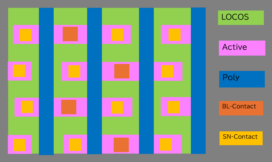
📐 Appendix A. Memory Cell Layout (Planar View)
Appendix A — Notes (Planar Layout)
This figure provides a simplified top-down (planar) layout view of a DRAM memory cell, illustrating the spatial relationship between:
- Active regions
- Word-line gate structures
- Bit-line contacts
- Isolation regions
🎯 Purpose of this appendix
- Not to define exact layer dimensions
- But to provide spatial context for process–failure interaction
Local process choices (plasma, cleaning, junction handling) act on
specific lateral regions, whose proximity strongly influences:
- Wafer test results
- Retention behavior
- Disturb sensitivity
- Yield and binning outcomes
🧱 Appendix B. Memory Cell Cross Section (Schematic)
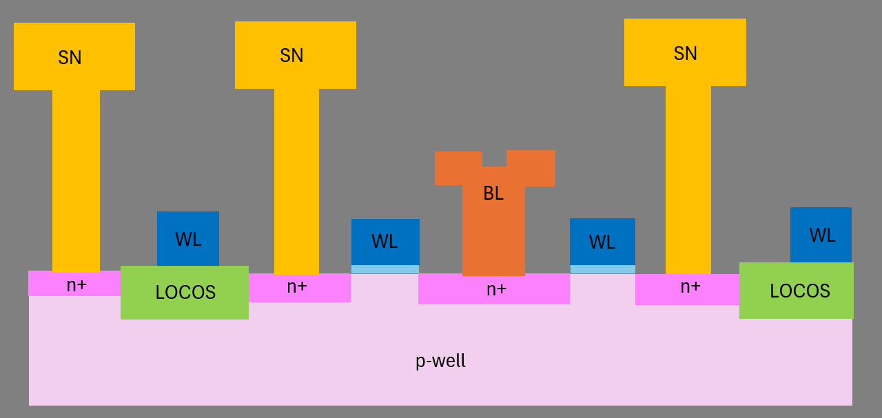
Appendix B — Notes (Cross Section)
This schematic shows a reconstructed vertical cross-sectional view of a representative 0.25µm-generation DRAM memory cell.
It highlights the relative positioning of:
- Active regions (n⁺ diffusion in p-well)
- Word-line (WL) gate stack
- Bit-line (BL) contact
- Storage node (SN)
- LOCOS-based isolation
⚠️ This is not a foundry-exact device profile.
It is an abstracted physical model for understanding
process–failure causality.
Mapping process sensitivities to structure
-
Gate etch plasma exposure
→ Junction damage beneath WL edges
→ Increased leakage, retention degradation -
Contact etch & post-clean
→ Leakage paths at BL–diffusion interface -
LOCOS edge geometry
→ Local electric-field enhancement
→ Disturb-related failures
Together with the planar layout, this cross-section enables lateral + vertical analysis of memory cell behavior.
🧠 Summary
This reconstructed process flow demonstrates how seemingly local process decisions—
- Plasma conditions
- Cleaning strategies
- Junction handling
propagated upward into:
- Wafer test binning behavior
- Retention and disturb failures
- Yield excursions
- Final product and business decisions
📘 This is the essence of a Legacy Process Case.