⏸ Pause Refresh Failure Physics
(0.25µm-generation DRAM)
This document describes the physical origin, manifestation, and evolution of Pause Refresh failures observed in 0.25µm-generation DRAM.
Pause refresh failure was the primary refresh-related reliability limiter for this technology node, dominating both yield and high-temperature reliability.
🧪 1. Failure Detection
Fail Bit Map Acquisition under Pause Stress
Pause refresh failure was first identified through fail bitmap acquisition under refresh-pause stress conditions.
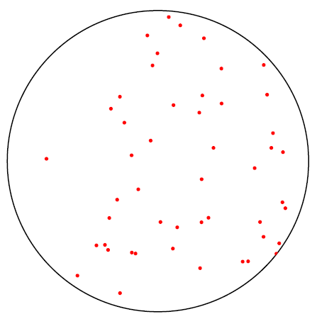
Fig. Fail bit distribution obtained under Pause Refresh stress in 0.25µm-generation DRAM
Observations
- Fail bits appeared spatially random
- No row-, column-, or block-level clustering
- No periphery or edge concentration
📌 Initial implication:
The failure was not driven by layout topology or array structure.
🔍 2. Failure Mode Identification
Single-Bit Dominant Behavior
Detailed bitmap analysis revealed:
- Failures occurred predominantly as isolated single-bit errors
- No word-line, bit-line, or block-level correlation
- No pattern-dependent aggregation
Mechanisms ruled out
| Excluded mechanism | Reason |
|---|---|
| Sense amplifier margin | No WL / BL correlation |
| Disturb coupling | No neighbor-dependent pattern |
| Systematic layout issue | No spatial regularity |
📌 Conclusion:
The dominant mechanism was intrinsic cell-level degradation.
🌡 3. Temperature Dependence
Failure Population Evolution
Temperature sweep testing showed:
- Fail bit count increased exponentially at high temperature
- Some failing bits recovered at lower temperature
- Fail population evolved continuously, not discretely
| Temperature | Behavior |
|---|---|
| Low T | Fail bits suppressed |
| Room T | Partial population visible |
| High T | Rapid population expansion |
📌 Key insight:
The failure mechanism was thermally activated and reversible,
indicating leakage-driven behavior, not permanent breakdown.
⚛️ 4. Physical Root Cause
n⁺ / p⁻ Junction Leakage
All observed characteristics are consistent with:
- n⁺ / p⁻ junction leakage current
- Shockley–Read–Hall (SRH) generation via defect states
- Strong exponential temperature dependence
💡 Critical finding
Storage capacitance (Ccell) margin was sufficient.
Retention loss was leakage-dominated, not C-limited.
This shifted engineering focus away from capacitor scaling toward junction integrity.
🧱 5. Device Structure Origin
Localized Leakage Paths
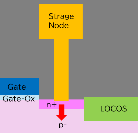
Fig. Local leakage paths responsible for Pause Refresh failures in 0.25µm-generation DRAM
Leakage was localized at:
- Junction periphery regions
- STI-adjacent diffusion edges
- High electric-field corners
📌 These locations are highly sensitive to process-induced damage.
⚙️ 6. Process Dependency
Plasma Damage Sensitivity
Strong correlation was observed between Pause failures and:
- Plasma etching exposure
- Aggressive ashing / dry cleaning
- Increased interface state density (Dit)
| Process factor | Electrical consequence |
|---|---|
| Plasma damage | Defect-assisted SRH leakage |
| Ashing stress | Junction edge degradation |
| Interface states | Temperature-accelerated leakage |
📌 Key lesson:
Process-induced latent damage surfaced only under pause stress.
🛠 7. Countermeasure Direction
Damage Avoidance, Not Circuit Compensation
Effective mitigation focused on preventing damage, not masking it:
- Plasma condition optimization
- Soft-landing etch techniques
- Ashing damage reduction
- Interface recovery anneals
These measures resulted in a significant reduction of Pause Refresh fail population at wafer level.
🧠 Summary — Failure Causality Chain
Pause Refresh failure in 0.25µm DRAM followed a clear, traceable chain:
Fail bitmap acquisition
→ Single-bit dominant failure mode
→ Strong temperature dependence
→ n⁺ / p⁻ junction leakage
→ Plasma damage–driven defect generation
📘 Legacy insight:
Reliability was limited not by design intent,
but by process-induced leakage physics.
This causal structure continues to reappear in modern memory technologies under different names.